Scanning drive circuit and flat-panel display device

A scanning driving circuit and scanning driving technology, applied in static indicators, instruments, etc., can solve the problems of reduced pixel aperture ratio, two scanning lines cannot be turned on at the same time, and scanning driving signals cannot meet pixel driving.

Inactive Publication Date: 2016-09-21
TCL CHINA STAR OPTOELECTRONICS TECH CO LTD
View PDF6 Cites 12 Cited by
  • Summary
  • Abstract
  • Description
  • Claims
  • Application Information

AI Technical Summary

Problems solved by technology

The large viewing angle performance of the VA mode is to divide each VA sub-pixel into a Main area and a Sub area. The Main area is the same as a normal sub-pixel. The Sub area generates a voltage difference with the Main area through various circuit designs to achieve a large viewing angle. However, pixels with this design often have two scan lines, where the first scan line normally charges the Main area and the Sub area of ​​the pixel, and the second scan line controls a thin film transistor to charge the Sub area. Charge sharing is used to realize the voltage difference between the pixel electrodes in the Main area and the Sub area. Since the two scanning lines will occupy a part of the space, resulting in a decrease in the pixel aperture ratio, the second scanning line and the scanning line of the next-level pixel are separated. Combined to increase the pixel aperture ratio, but such a design requires that the two scan lines cannot be turned on at the same time, otherwise the Main area and the Sub area cannot generate a voltage difference. In the existing large-size panel scanning drive circuit design, due to factors such as circuit load, often Multiple clock signals of 4CK, 6CK or 8CK are used. The scan driving signal generated by such a circuit cannot meet the above-mentioned pixel driving requirements. Therefore, the above problems need to be improved urgently.

Method used


Image

  • Scanning drive circuit and flat-panel display device
  • Scanning drive circuit and flat-panel display device
  • Scanning drive circuit and flat-panel display device

Examples


Embodiment Construction

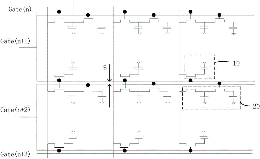
[0031] see figure 1 , is a circuit diagram of a scan driving circuit of a VA mode liquid crystal panel in the prior art. In order to improve the large viewing angle display characteristics of the panel in VA mode, charge sharing is a very common design. The pixel equivalent circuit using this design is as follows: figure 1 shown. figure 1Shown in the two dotted line boxes in is the Main region 10 and the Sub region 20 of a sub-pixel, wherein each of the Main region 10 and the Sub region 20 charges the pixel electrode by a thin film transistor, and the gate of the thin film transistor in the Main region 10 The gates of a thin film transistor in the Sub area 20 are connected to the first scanning line Gate (n+1), and the other thin film transistor in the Sub area 20 is also connected to the second scanning line Gate (n+2). When the second scanning line Gate (n+2) is turned on, another thin film transistor in the Sub region 20 can perform a charge sharing action on the Sub regi...


PUM


Abstract

The invention discloses a scanning drive circuit and a flat-panel display device. The scanning drive circuit comprises a plurality of cascaded scanning drive units, wherein each scanning drive unit comprises an input circuit, an output circuit, a control circuit and a scanning line; each input circuit is used for receiving an upper-stage stage transmission signal as well as first and second clock signals, and outputting a current-stage stage transmission signal and a pull-up control signal; each output circuit is used for receiving signals from the corresponding input circuit, and outputting a lower-stage stage transmission signal; each control circuit is used for receiving first and second pull-down signals as well as the pull-up control signal and outputting a scanning drive signal, or receiving the first clock signal, the upper-stage stage transmission signal, a third clock signal as well as the pull-up control signal and outputting the scanning drive signal; and each scanning line is used for receiving the scanning drive signal and controlling a pixel unit. Therefore, the effects of satisfying driving requirements of charge-shared pixels while ensuring high aperture opening ratio of the charge-shared pixels without affecting the operation reliability of the scanning drive circuit are achieved.

Description

technical field [0001] The invention relates to the field of display technology, in particular to a scan driving circuit and a flat display device. Background technique [0002] The VA (Vertical Alignment, Vertical Alignment) liquid crystal mode has the advantages of high contrast, fast response time and high transmittance, and has been widely used. The large viewing angle performance of the VA mode is to divide each VA sub-pixel into a Main area and a Sub area. The Main area is the same as a normal sub-pixel. The Sub area generates a voltage difference with the Main area through various circuit designs to achieve a large viewing angle. However, pixels with this design often have two scan lines, where the first scan line normally charges the Main area and the Sub area of ​​the pixel, and the second scan line controls a thin film transistor to charge the Sub area. Charge sharing is used to realize the voltage difference between the pixel electrodes in the Main area and the S...

Claims


Application Information

Patent Timeline
Patent Type & Authority Applications(China)
IPC IPC(8): G09G3/36
CPCG09G3/3677G09G3/3659G09G2300/0447G09G2300/0465G09G2310/0205G09G2310/0286G09G3/36G09G2310/08
Inventor 杜鹏
Owner TCL CHINA STAR OPTOELECTRONICS TECH CO LTD
Why Eureka
Try Eureka