Three-dimensional winding inductor, transformer, equalizer and LC filter
A wire-wound inductance, three-dimensional technology, applied in the field of inductance, achieves high reliability, great practical significance and practical value, and shortens the production cycle of products.
- Summary
- Abstract
- Description
- Claims
- Application Information
AI Technical Summary
Problems solved by technology
Method used
Image

Examples
Embodiment 1
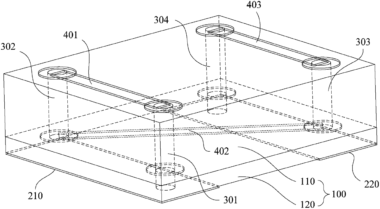
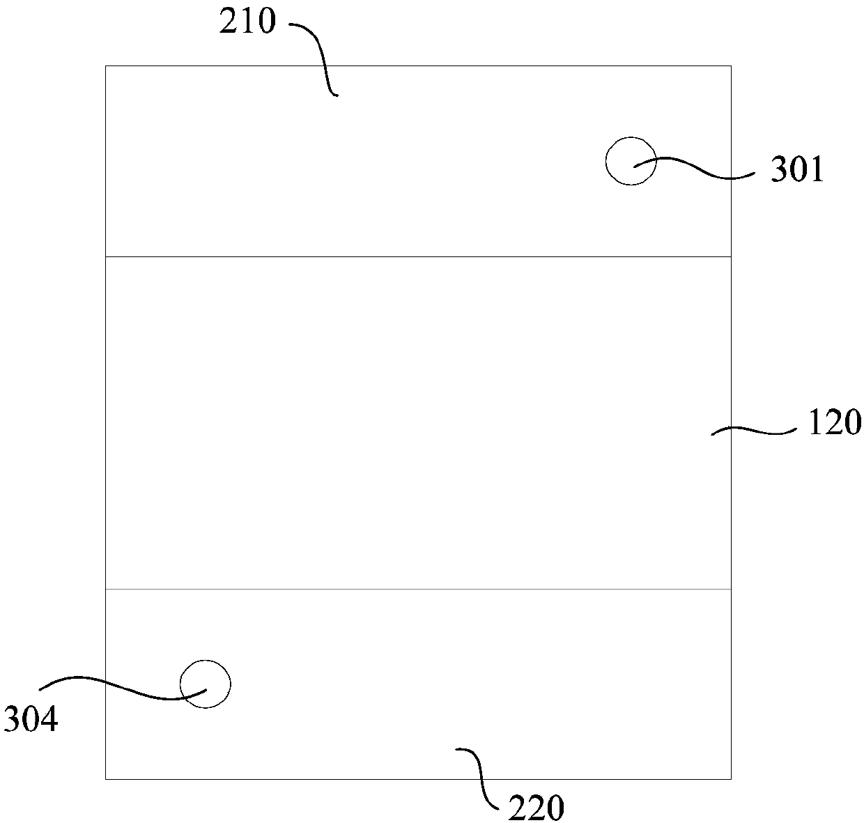
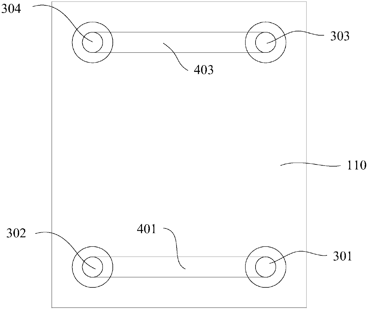
[0038] see Figure 1 to Figure 3 , in this embodiment, the three-dimensional wire-wound inductor is a three-dimensional wire-wound inductor with two layers and two turns. The three-dimensional wound inductor includes a PCB (Printed Circuit Board, printed circuit board) 100 , an input pad 210 , an output pad 220 , four conductive channels 301 - 304 and three inductor coil wires 401 - 403 . Wherein, the PCB board 100 is a double dielectric layer PCB board, including a first dielectric layer 110 and a second dielectric layer 120 . The conductive channels 301 - 304 all pass through the first dielectric layer 110 and the second dielectric layer 120 of the PCB 100 . The inductor coil wires 401 - 403 are respectively disposed on the first dielectric layer 110 and the second dielectric layer 120 of the PCB 100 . Moreover, each inductor coil wire is located on the same dielectric layer, and the two ends of each inductor coil wire are respectively connected to two conductive channels....
Embodiment 2
[0044] see Figure 4 and Figure 5 , in this embodiment, the three-dimensional winding inductor is a two-layer four-turn three-dimensional winding inductor. The three-dimensional wound inductor includes a PCB (Printed Circuit Board, printed circuit board) 100 , an input pad 210 , an output pad 220 , eight conductive channels 301 - 308 and seven inductor coil wires 401 - 407 . Wherein, the PCB board 100 is a double dielectric layer PCB board, including a first dielectric layer 110 and a second dielectric layer 120 . The conductive channels 301 - 308 all penetrate the first dielectric layer 110 and the second dielectric layer 120 of the PCB 100 . The inductor coil wires 401 - 407 are respectively disposed on the first dielectric layer 110 and the second dielectric layer 120 of the PCB 100 . In addition, each inductor coil wire is located on the same dielectric layer, and the two ends of each inductor coil wire are respectively connected to two conductive channels. All the in...
Embodiment 3
[0051] see Figure 6 and Figure 7 The difference between the three-dimensional wire-wound inductor in this embodiment and the three-dimensional wire-wound inductor in Embodiment 2 lies in: the middle pad 500 . The middle pad 500 is disposed on the surface of the PCB 120 and located between the input pad 210 and the output pad 220 . The middle pad 500 is connected to the inductor coil wire through a conductive path.
[0052] Specifically, in this embodiment, the surface of the first dielectric layer 110 away from the second dielectric layer 120 is set as the first surface of the first dielectric layer 110 . The inductor coil wire 401 , the inductor coil wire 403 , the inductor coil wire 405 and the inductor coil wire 407 are disposed on the first surface of the first dielectric layer 110 . The inductor wire 402 , the inductor wire 404 and the inductor wire 406 are disposed between the first dielectric layer 110 and the second dielectric layer 120 . The input pad 210 is con...
PUM
| Property | Measurement | Unit |
|---|---|---|
| q value | aaaaa | aaaaa |
Abstract
Description
Claims
Application Information
 - R&D
- Intellectual Property
- Life Sciences
- Materials
- Tech Scout
- Unparalleled Data Quality
- Higher Quality Content
- 60% Fewer Hallucinations
Browse by: Latest US Patents, China's latest patents, Technical Efficacy Thesaurus, Application Domain, Technology Topic, Popular Technical Reports.
© 2025 PatSnap. All rights reserved.Legal|Privacy policy|Modern Slavery Act Transparency Statement|Sitemap|About US| Contact US: help@patsnap.com