Manufacturing method for embedded type circuit of PCB (Printed Circuit Board)

A manufacturing method and embedded technology, applied in printed circuit manufacturing, printed circuits, electrical components, etc., can solve the problems of low circuit fineness and poor uniformity, and achieve stable embedded circuits, a wide range of applications, and improved integration. Effects of Density and Stability

Active Publication Date: 2016-09-21
AKM ELECTRONICS TECH SUZHOU
View PDF4 Cites 18 Cited by
  • Summary
  • Abstract
  • Description
  • Claims
  • Application Information

AI Technical Summary

Problems solved by technology

[0004] The defect of the prior art is that both the semi-additive method and the subtractive method need to use the film dry film for the steps of image exposure and development, so it is limited by the film dry film, the fineness of the circuit is low, and the uniformity is low. Poor, and the H / W value is often less than 1.0

Method used


Image

  • Manufacturing method for embedded type circuit of PCB (Printed Circuit Board)
  • Manufacturing method for embedded type circuit of PCB (Printed Circuit Board)

Examples


Embodiment 1

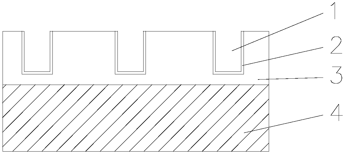
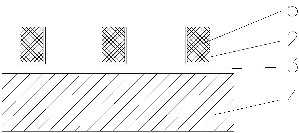
[0049] see figure 1 and figure 2, a method for manufacturing a PCB embedded circuit, comprising the following steps:

[0050] 1) Construct the motherboard

[0051] 1a) Clean the wafer with piranha solution at 100°C for 15 minutes, then clean it with deionized water, and then dry it.

[0052] 1b) Preheat the wafer at 115°C for 1 min.

[0053] 1c) The photoresist is then spin-coated on the wafer at a rotation speed of 2500 rpm for 30 s, and then baked at 110° C. for 1 min to remove the solvent in the photoresist.

[0054] 1d) Design a photomask according to the required circuit pattern, cover the photomask on the wafer, and then expose to UV light for 5-10s. In this embodiment, the line width and line spacing of the circuit pattern are both 2 µm, and the copper thickness is 2 µm.

[0055] 1e) Dip the wafer in the developer solution for 1 min, rinse it with deionized water, and dry it.

[0056] 1f) Etching the wafer obtained in step 1e), controlling the etching rate to 0.5...

Embodiment 2

[0081] see figure 1 and figure 2 , a method for manufacturing a PCB embedded circuit, comprising the following steps:

[0082] 1) Construct the motherboard

[0083] 1a) Clean the wafer with piranha solution at 125°C for 20 minutes, then clean it with deionized water, and then dry it.

[0084] 1b) Preheat the wafer at 115°C for 3 minutes.

[0085] 1c) The photoresist is then spin-coated on the wafer at a rotation speed of 3000 rpm for 30 s, and then baked at 110° C. for 1.5 min to remove the solvent in the photoresist.

[0086] 1d) Design a photomask according to the required circuit pattern, cover the photomask on the wafer, and then expose to UV light for 5-10s. In this embodiment, the line width and line spacing of the circuit pattern are both 10 µm, and the copper thickness is 20 µm.

[0087] 1e) Dip the wafer in the developer solution for 1.5 min, rinse it with deionized water, and dry it.

[0088] 1f) Etching the wafer obtained in step 1e), controlling the etching ...

Embodiment 3

[0113] see figure 1 and figure 2 , a method for manufacturing a PCB embedded circuit, comprising the following steps:

[0114] 1) Construct the motherboard

[0115] 1a) Clean the wafer with piranha solution at 150°C for 25 minutes, then clean it with deionized water, and then dry it.

[0116] 1b) Preheat the wafer at 115°C for 5 minutes.

[0117] 1c) The photoresist is then spin-coated on the wafer at a rotation speed of 3500 rpm for 30 s, and then baked at 110° C. for 2 min to remove the solvent in the photoresist.

[0118] 1d) Design a photomask according to the required circuit pattern, cover the photomask on the wafer, and then expose to UV light for 5-10s. In this embodiment, the line width and line spacing of the circuit pattern are both 80 μm, and the copper thickness is 200 μm.

[0119] 1e) Dip the wafer in the developer solution for 2 minutes, then rinse it with deionized water, and dry it.

[0120] 1f) Etching the wafer obtained in step 1e), controlling the et...


PUM


Abstract

The invention discloses a manufacturing method for an embedded type circuit of a PCB (Printed Circuit Board). The method comprises the following steps of firstly, constructing a mother board whose surface is provided with a concave preset circuit pattern; secondly, constructing a pattern transfer daughter board whose surface is provide with a circuit pattern protection; thirdly, utilizing the pattern transfer daughter board and ultraviolet curing optical cement to construct a circuit carrier on a circuit board substrate through a rolling way in order to obtain a circuit pattern groove on the circuit carrier; fourthly, manufacturing a conductive seed layer on the inner surface of the circuit pattern groove; and lastly, carrying out copper plating on the conductive seed layer of the circuit pattern groove and filling the circuit pattern groove through a copper layer generated in a copper plating process in order to obtain the embedded type circuit which is embedded into the circuit carrier. According to the manufacturing method for the embedded circuit of the PCB, the manufactured embedded circuit both has a higher H / W value (greater than 1) and small line width and line spacing (the minimum values of the line width and the line spacing both reach 2 microns) so as to help to improve the integration density and the stability of the printed circuit board remarkably.

Description

technical field [0001] The invention relates to the technical field of printed circuits, in particular to a method for manufacturing embedded circuits of a printed circuit board (PCB, Printed Circuit Board). Background technique [0002] The current development of electronic products is very rapid, and technology updates are changing with each passing day, which puts forward more and more stringent requirements for product integration density and process precision in the PCB industry. Among them, the PCB circuit part is a very critical component. The accuracy, conductivity and stability of the circuit play an important role in the construction of thin, fast response, and versatile electronic devices. The line aspect ratio H / W (line height / line width) is a very important concept in the construction of fine lines, because a larger H / W value means lower resistance and higher line density And better heat dissipation performance. [0003] There are two common methods for tradit...

Claims


Application Information

Patent Timeline
Patent Type & Authority Applications(China)
IPC IPC(8): H05K3/12
CPCH05K3/125H05K3/1258H05K2203/013H05K2203/052
Inventor 张仕通崔成强王锋伟柴志强潘丽
Owner AKM ELECTRONICS TECH SUZHOU
Why Eureka
Try Eureka