Method for manufacturing high-density interconnection circuit board

A technology for high-density interconnection and circuit boards, which is applied in the fields of printed circuit, multilayer circuit manufacturing, and printed circuit manufacturing. It can solve problems such as process scrapping, low production efficiency, and client scrapping. The effect of high efficiency and alignment accuracy

Inactive Publication Date: 2021-05-04
HUIZHOU KING BROTHER CIRCUIT TECH
View PDF7 Cites 2 Cited by
  • Summary
  • Abstract
  • Description
  • Claims
  • Application Information

AI Technical Summary

Problems solved by technology

[0003] 1. The manufacturing process of high-layer high-density interconnection circuit board products is cumbersome and complicated, and the production efficiency is low;
[0004] 2. The alignment accuracy between layers is insufficient during the production of high-multilayer high-density interconnection circuit board products, which is prone to process scrapping;
[0005] 3. The reliability of the product cannot be fully guaranteed, and it is easy to cause the client to be scrapped

Method used


Image

  • Method for manufacturing high-density interconnection circuit board

Examples


Embodiment Construction

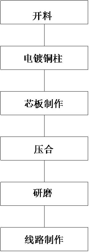
[0030]In order to make the above objects, features, and advantages of the present invention, the specific embodiments of the present invention will be described in detail below with reference to the accompanying drawings. Many specific details are set forth in the following description to fully understand the present invention. However, the present invention can be implemented in many other fails there are many otherwise described herein, and those skilled in the art may do similar improvements without departing from the connotation of the present invention, and thus the present invention is not limited by the specific embodiments disclosed below.

[0031]It should be noted that when a component is considered to be "connected" another element, it can be directly connected to another element or may exist at the same time. In contrast, when the element is called "direct" to connect to another element, there is no intermediate element.

[0032]All techniques and scientific terms used herein ...


PUM


Abstract

The invention discloses a method for manufacturing a high-density interconnection circuit board. The method comprises the steps of S1, cutting, S2, copper column electroplating, S3, core board manufacturing, S4, pressing, S5, grinding and S6, circuit manufacturing. According to the method for manufacturing the high-density interconnection circuit board, the manufacturing method is simple, conduction of any layer can be achieved, and the production efficiency is improved; and the method for electroplating the copper column has the advantages of no generation of recesses, easy realization of a structure of combining holes on holes and hole discs, high alignment precision, and realization of accurate control of the copper thickness of each layer of circuit by adopting a semi-additive method to manufacture the pattern circuit, realization of more precise circuit manufacture, and guarantee of the product quality.

Description

Technical field[0001]The present invention relates to the technical field of PCB plate making, in particular a method for making a high density interconnect circuit board.Background technique[0002]The PCB (Printed Circuit Board), the Chinese name is a printed circuit board, also known as the printed circuit board, is an important electronic component, is a support of the electronic component, and is an electrical connection of electronic components. Since it is made of electronic printing, it is called a "print" circuit board. The high-density interconnect circuit board conventional conduction process is to use a drilling + electroplating to achieve an inter-stationary, which has the following shortcomings for making high-multi-layer high-density interconnect circuit board products:[0003]1. High-multi-layer high-density interconnect line board product process is cumbersome, low production efficiency;[0004]2, high-multi-layer high-density interconnect line board product production is...

Claims


Application Information

Patent Timeline
Patent Type & Authority Applications(China)
IPC IPC(8): H05K3/42H05K3/46
CPCH05K3/429H05K3/4611H05K2203/061
Inventor 杨贵李波樊廷慧田政权黄双双肖鑫叶湘明
Owner HUIZHOU KING BROTHER CIRCUIT TECH
Why Eureka
Try Eureka