Optical function device with photonic band gap and/or filtering characteristics

a technology of optical function and filtering characteristics, which is applied in the field of stacking materials, can solve the problems of affecting the quality of crystals, the inability to manufacture such a stacking structure, and the inability to use amorphous materials in semiconductor devices except for solar cells, so as to achieve the effect of reducing the manufacturing cos

Inactive Publication Date: 2002-04-30
SHIN-ETSU HANDOTAI CO LTD
View PDF4 Cites 50 Cited by
  • Summary
  • Abstract
  • Description
  • Claims
  • Application Information

AI Technical Summary

Benefits of technology

The use of a smart cut method as the substrate bonding method is advantageous in that the stacked material can be more efficiently and more accurately fabricated.
Thus, layers having different refractive indexes can be bonded in the thickness direction, as is the case of the aforementioned substrate bonding method, thereby making it possible to fabricate the photonic band gap stacked structures 10, 10a and the stacked structures 11, 11a having the filtering characteristic in a similar manner.

Problems solved by technology

However, a stacked structure exhibiting the photonic band gap characteristic is composed of two layers having different crystal structures such as a semiconductor material and an insulating material or crystal and amorphous, so that it has been difficult to fabricate such a stacked structure by the vapor phase growth method while maintaining the planarity of the interface and the integrity of crystal structures.
The amorphous material, however, is not used in semiconductor devices except for solar cells.
Therefore, this method may cause a problem when crystal silicon is required.
However, since a heat treatment is used for bonding, the quality of crystal may be problematic.
While several other examples have also been reported, all of them still leave unsolved problems of the quality of stacked crystal, the uniformity of periodic structure and so on.

Method used


Image

  • Optical function device with photonic band gap and/or filtering characteristics
  • Optical function device with photonic band gap and/or filtering characteristics
  • Optical function device with photonic band gap and/or filtering characteristics

Examples


examples 2-4

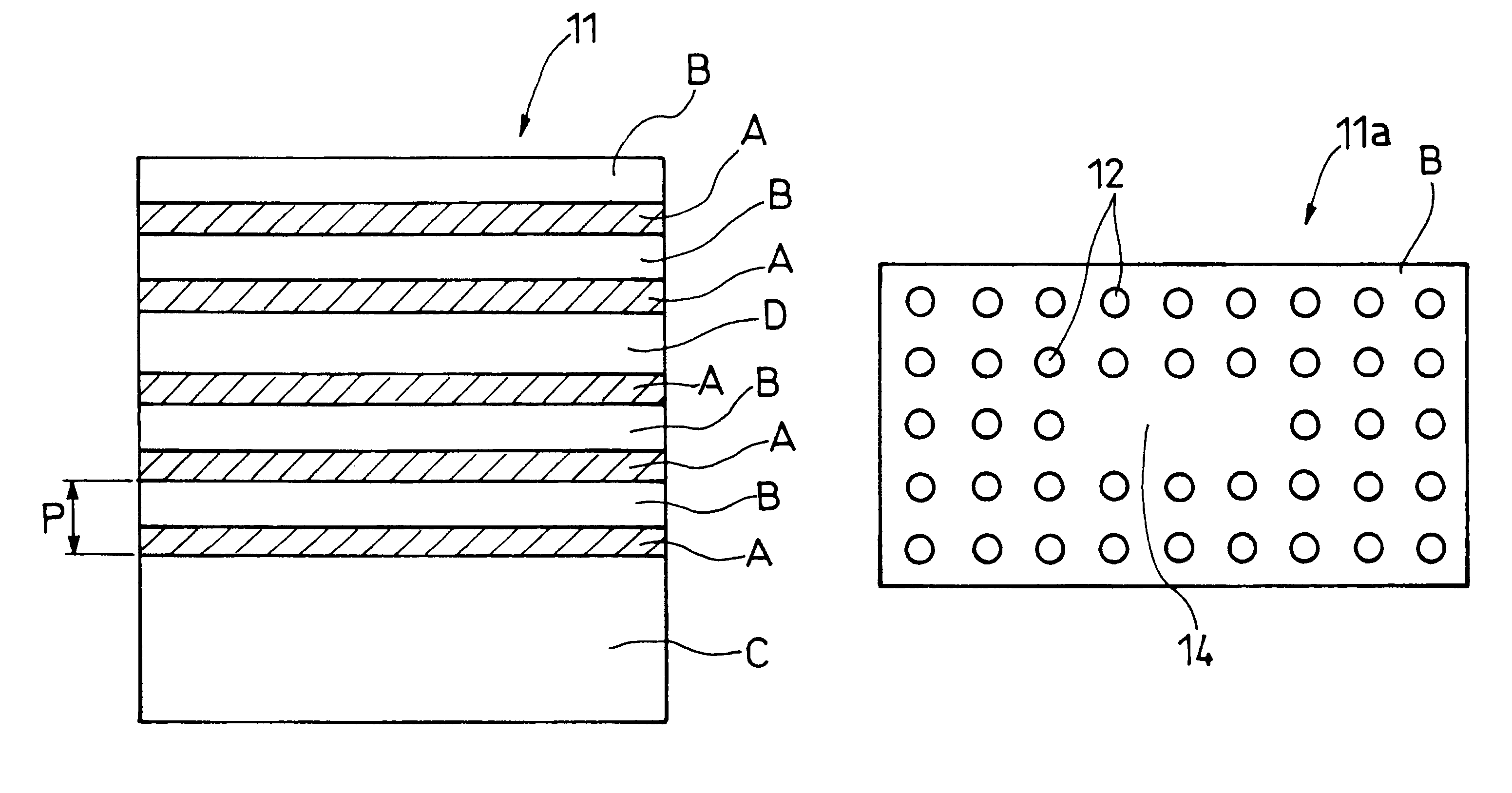
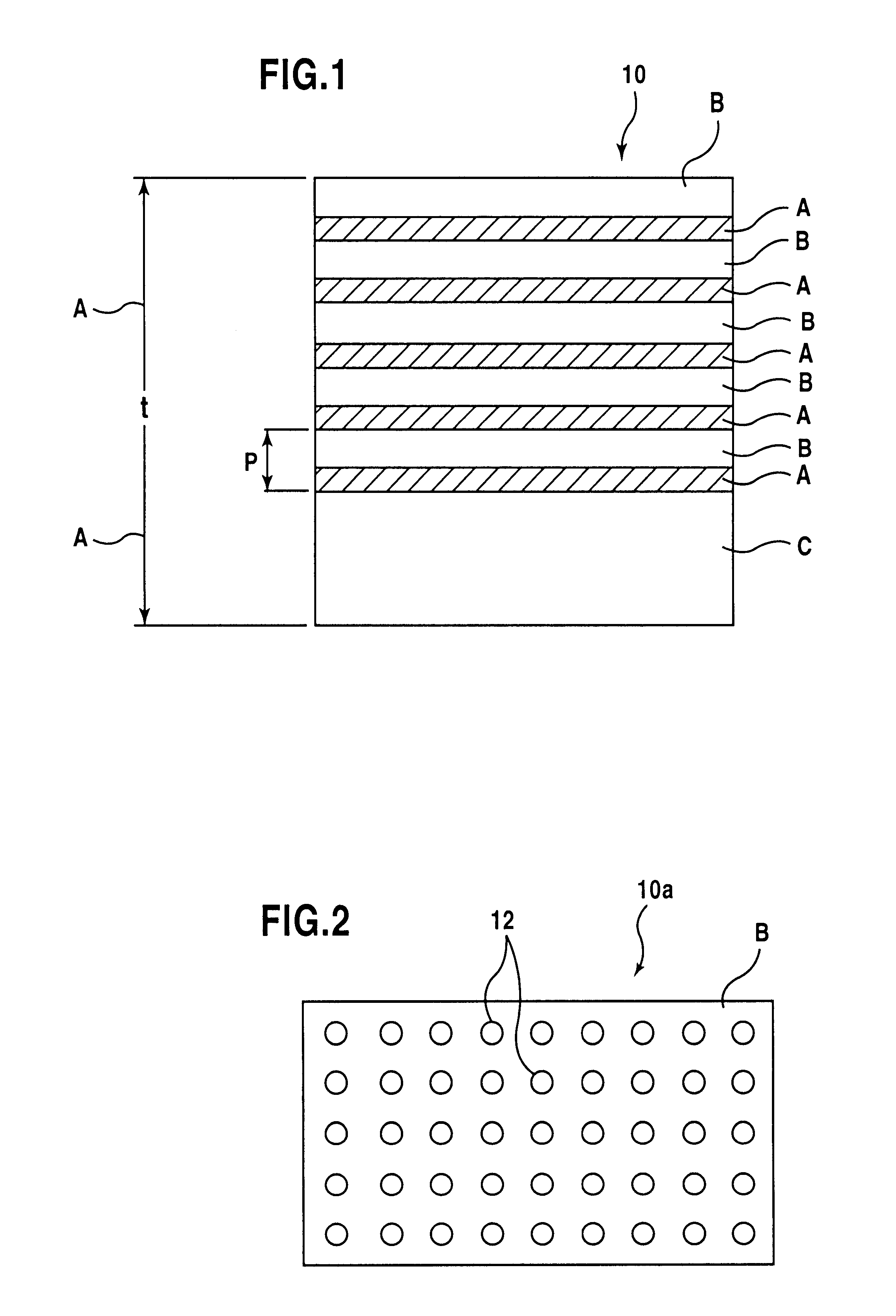
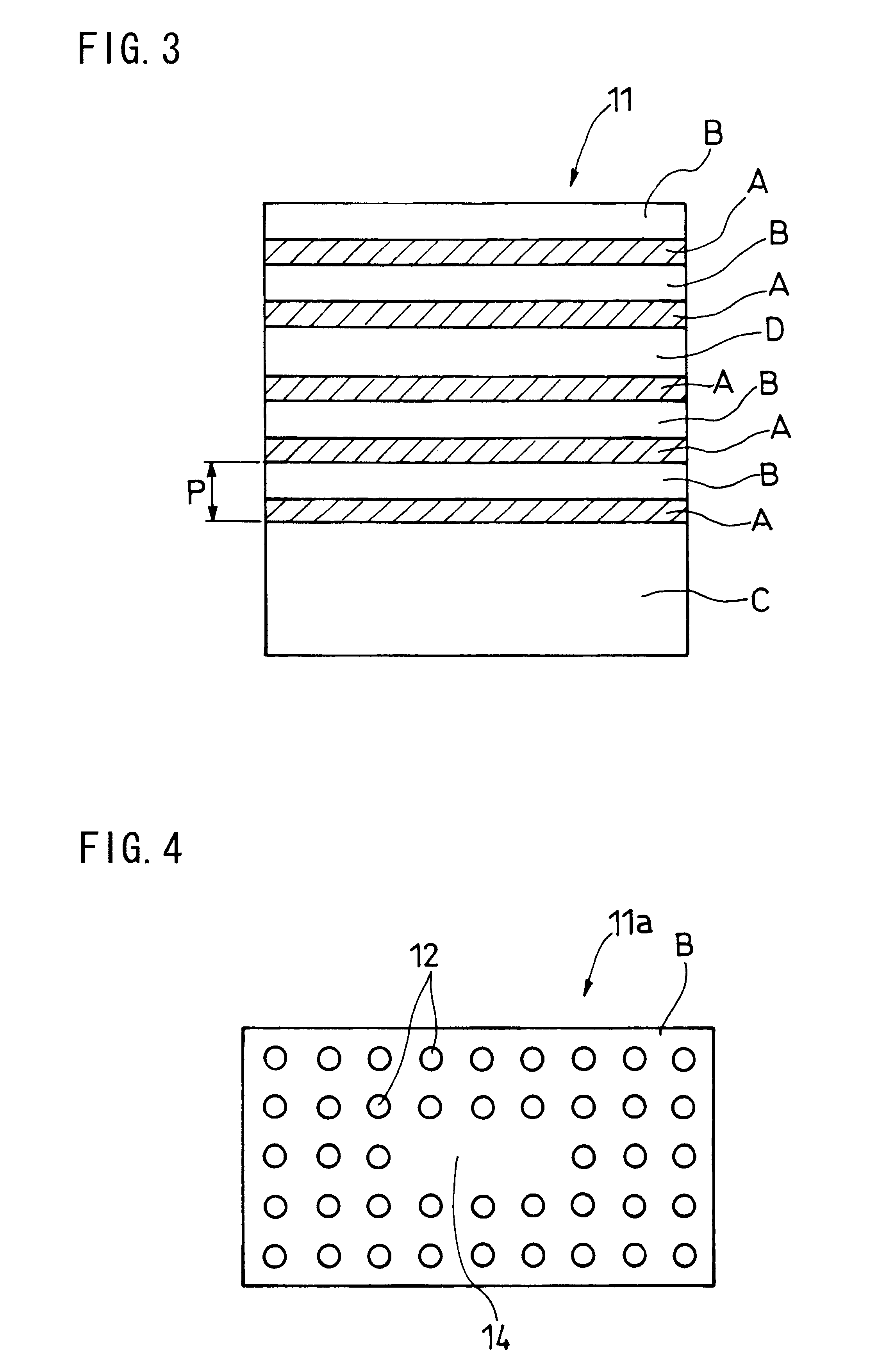
An insulating layer (A) and a silicon layer (B) were stacked alternately on a silicon substrate (C) several times to fabricate a photonic band gap structure in the thickness direction.

The silicon layer had a thickness of 400 nm, while the insulating layer also had a thickness of 400 nm, and these alternate layers were stacked five times, i.e., the number of periods was five. A silicon oxide film (Example 2) or a silicon nitride film (Example 3) was used as the insulating layer. When light was directed to the stacked structure from a direction perpendicular thereto to measure a transmission characteristic, the stacked structure exhibited the transmittance of zero over a wavelength band ranging from one to two microns, with the silicon oxide film (example 2), thus confirming that a photonic band gap structure is provided.

It was also confirmed that with the silicon nitride film (Example 3), the photonic band gap characteristic was exhibited over substantially a similar wavelength range...

examples 5 and 6

An insulating layer (A) and a compound semiconductor layer (B) were stacked alternately on a silicon substrate (C) several times to fabricate a photonic band gap structure in the thickness direction.

The compound semiconductor layer had a thickness of 400 nm, while the insulating layer also had a thickness of 400 nm, and these alternate layers were stacked five times, i.e., the number of periods was five. GaAs was used as the compound semiconductor layer. A silicon oxide film (Example 5) or a silicon nitride film (Example 6) was used as the insulating layer. It was confirmed that the stacked structure exhibited the transmittance of zero over a wavelength band ranging from one to two microns, when the silicon oxide film was used (Example 5), and accordingly a photonic band gap structure was provided. It was also confirmed that with the silicon nitride film (Example 6), the photonic band gap characteristic was exhibited over substantially a similar wavelength range.

examples 7-11

Holes were formed at regular intervals through each of the stacked structures described above in Examples 2-6. The holes had a diameter of 400 nm and were formed at intervals of 800 nm. It was confirmed that the transmittance was zero over a wavelength band ranging from one to two microns with respect to the light transmission characteristic in the in-plane direction of the stacked structure. As a result, a three-dimensional photonic band gap can be realized in the stacked structure which exhibits the transmittance of zero over this wavelength band when light is incident on the stacked structure from any direction.

As described above, the stacked material in accordance with the present invention is advantageous in that it is free from a degraded quality of crystal, formed with a precise periodicity, fabricated without relying on the vapor phase growth method, and utilized as an optical function device. Also advantageously, the optical function device in accordance with the present in...


PUM


Abstract

A stacked material free from a degraded quality of crystal, formed with a precise periodicity, and fabricated without relying on the vapor phase growth method is provided. An optical function device using the stacked material is also provided. A starting stacked material composed of two alternate layers (A), (B) having different refractive indexes is stacked over two periods or more by a substrate bonding method to provide a multi-periodic stacked structure.

Description

1. Field of the InventionThe present invention relates to a stacked material which exhibits a photonic band gap characteristic or a filtering characteristic and a light emitting characteristic, and an optical function device using the stacked material.2. Description of the Related ArtThe photonic band gap is a function for limiting the transmittance of light at a particular wavelength by periodically stacking two kinds of materials (A), (B) having different refractive indexes over two or more periods. For example, as illustrated in FIG. 1, the photonic band gap can be realized by periodically stacking a starting stacked structure composed of two layers (A), (B) having different refractive indexes over two or more periods on a substrate (C).The filtering characteristic, on the other hand, is realized by inserting a layer region (D) having a different thickness from that of the layer (A) or the layer (B) into a portion of the stacked structure of the photonic band gap, for example, as...

Claims


Application Information

Patent Timeline
Patent Type & Authority Patents(United States)
IPC IPC(8): G02B6/12G02B6/122G01J1/02G02B5/28H01L21/02H01L27/12H01L31/02H01S3/16
CPCB82Y20/00G02B6/1225G02B6/12
Inventor ABE, TAKAOAGA, HIROJI
Owner SHIN-ETSU HANDOTAI CO LTD
Why Eureka
Try Eureka