Substrate dicing method

Inactive Publication Date: 2000-11-28
THERMOCARBON
View PDF35 Cites 50 Cited by
  • Summary
  • Abstract
  • Description
  • Claims
  • Application Information

AI Technical Summary

Problems solved by technology

Increasing use of microelectronic technology in microwave and hybrid circuits, memories, computers, defense and medical electronics has created an array of new and difficult problems for the industry.
More expensive and exotic materials, such as sapphire, garnet, alumina, ceramic, glass, quartz, ferrite, and other hard, brittle substrates, are being used.
They are often combined to produce multiple layers of dissimilar materials, thus adding further to the dicing problems.
The high cost of these substrates, together with the value of the circuits fabricated on them, makes it difficult to accept anything less than high yield at the die-separation phase.
Because of the diamond dicing blade's extreme fineness, compliance with a strict set of parameters is imperative, and even the slightest deviation from the norm could result in complete failure.
Because most state-of-the-art dicing equipment has been designed specifically to dice silicon wafers, problems arise when it is necessary to cut harder and/o

Method used


Image

  • Substrate dicing method
  • Substrate dicing method
  • Substrate dicing method

Examples


Embodiment Construction

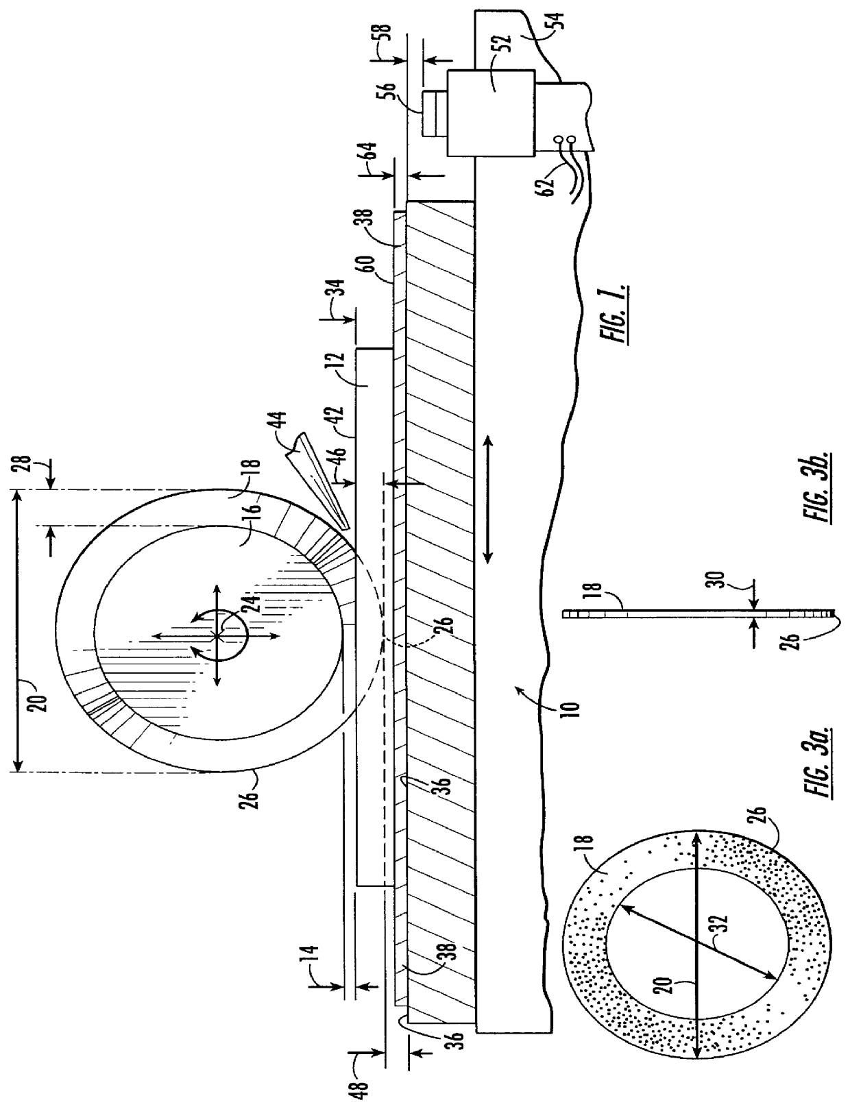
The present invention will now be described more fully hereinafter with reference to the accompanying drawings, in which preferred embodiments of the invention are shown. This invention may, however, be embodied in many different forms and should not be construed as limited to the embodiments set forth herein. Rather, these embodiments are provided so that this disclosure will be thorough and complete, and will fully convey the scope of the invention to those skilled in the art. Like numbers refer to like elements throughout.

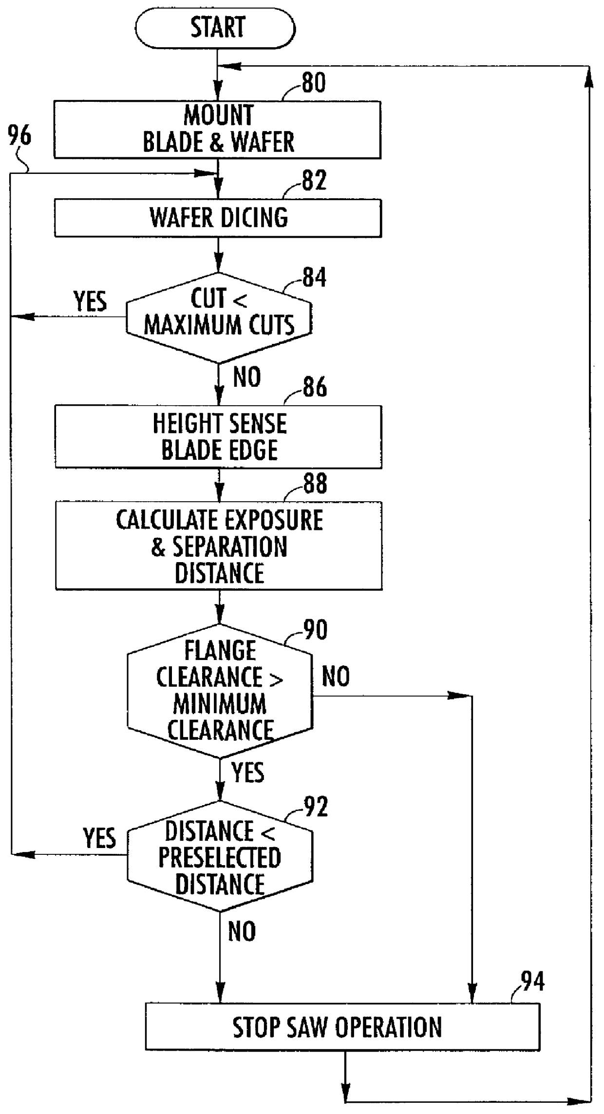
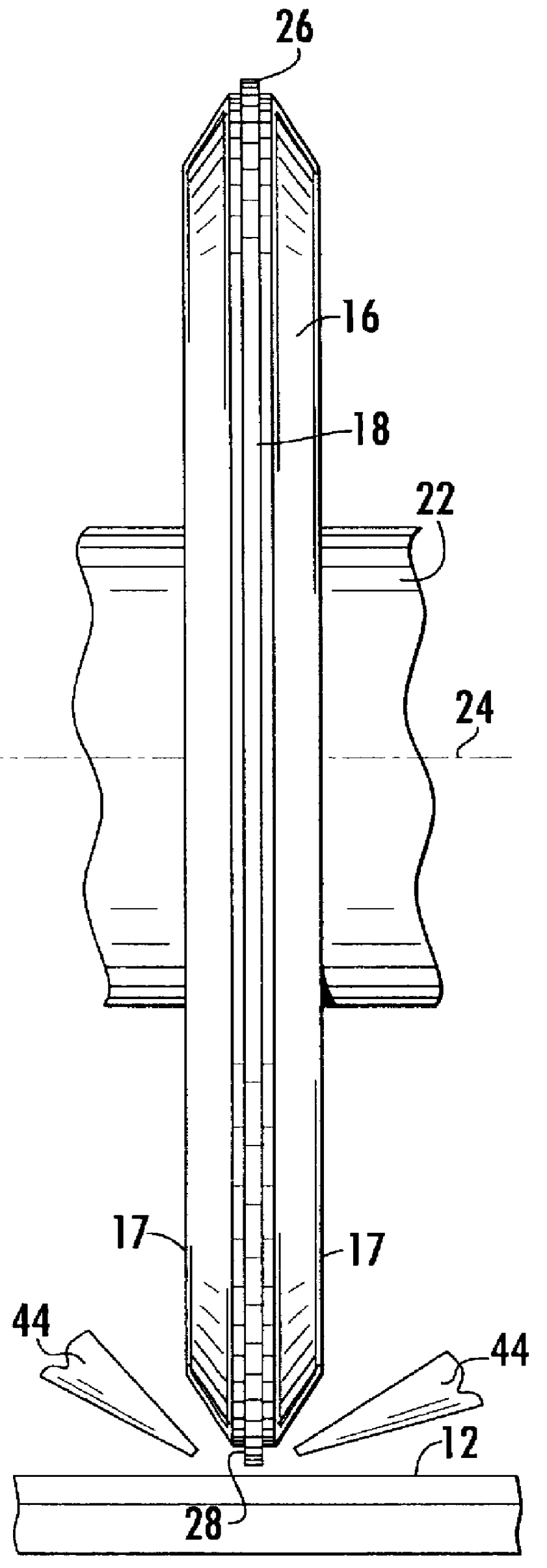
The preferred embodiment of the present invention is described with reference to the drawings, wherein a method and system 10 for automatically dicing a semiconductor wafer or a substrate 12, herein described by way of example, provides a safe clearance 14 between a dicing blade flange 16 and the substrate 12, as illustrated with reference to FIG. 1. By way of example, a resin-bonded dicing blade 18 will wear or reduce in diameter 20 as it is used to cut various...


PUM

PropertyMeasurementUnit
Angleaaaaaaaaaa
Angleaaaaaaaaaa
Diameteraaaaaaaaaa

Abstract

A programmable dicing saw is operable with movement of its spindle and work surface for aligning a dicing blade juxtaposed between flanges on the spindle and dicing a substrate along a predetermined blade path. By locating the center of the substrate, an efficient movement of the blade relative to the substrate center rather than the work surface center saves time. Locating the center of the blade includes aligning opposing substrate edges and edge location data entry into a processor for calculation of the substrate center and control based on the substrate center. In addition, prior to cutting along the edges of the substrate, the dicing blade is first aligned for travel parallel to and proximate the edge of the substrate, and an alignment offset is provided to the programmable dicing saw for laterally moving the blade toward the center of the substrate prior to making a cut and avoiding damage to the blade and substrate that typically results when the blade slides along the substrate edge rather than cutting into the substrate. In addition, by knowing the substrate center location, an arcuate cut can be accurately made into the substrate by making multiple straight cuts with a rotation of the substrate about its center between each cut. A flange clearance is monitored by measuring the blade exposure after a preselected number of cuts during the substrate dicing, and a minimum flange clearance permitted before blade movement toward the substrate is automatically stopped.

Description

BACKGROUND OF INVENTION1. Field of InventionThe invention relates generally to the dicing of semiconductor wafers and, more particularly to the monitoring of blade location and flange clearance for safely cutting a semiconductor wafer.2. Background ArtDie separation, or dicing, by sawing is the process of cutting a microelectronic substrate into its individual circuit die with a rotating circular abrasive saw blade. This process has proven to be the most efficient and economical method in use today. It provides versatility in selection of depth and width (kerf) of cut, as well as selection of surface finish, and can be used to saw either partially or completely through a wafer or substrate.Wafer dicing technology has progressed rapidly, and dicing is now a mandatory procedure in most front-end semiconductor packaging operations. It is used extensively for separation of die on silicon integrated circuit wafers. Increasing use of microelectronic technology in microwave and hybrid circ...

Claims


Application Information

Patent Timeline
IPC IPC(8): B23D59/00B24B27/06B24B49/18B24B49/00B28D5/00B28D5/02
CPCB23D59/002B28D5/022B24B49/183B24B27/06
Inventor BOUCHER, JOHN N.BAJUNE, DAVID E.
Owner THERMOCARBON
Why Eureka
Try Eureka