Method and apparatus for converting precursor layers into photovoltaic absorbers

a technology of photovoltaic absorbers and precursor layers, which is applied in the direction of semiconductor devices, coatings, chemical vapor deposition coatings, etc., can solve the problems of high equipment cost, low material utilization, and high cost of equipment, and achieve low throughput, low material utilization, and high equipment cost

Inactive Publication Date: 2007-05-17
SOLOPOWER
View PDF9 Cites 103 Cited by
  • Summary
  • Abstract
  • Description
  • Claims
  • Application Information

AI Technical Summary

Benefits of technology

[0007] The first technique that yielded high-quality Cu(In,Ga)Se2 films for solar cell fabrication was co-evaporation of Cu, In, Ga and Se onto a heated substrate in a vacuum chamber. However, low materials utilization, high cost of equipment, difficulties faced in large area deposition and relatively low throughput are some of the challenges faced in commercialization of the co-evaporation approach.
[0008] Another technique for growing Cu(In,Ga)(S,Se)2 type compound thin films for solar cell applications is a two-stage process where metallic com

Problems solved by technology

However, the cost of electricity generated using silicon-based solar cells is higher than the cost of electricity generated by the more traditional methods.
However, low materials utilization, high cost of equipment, difficulties faced in large area deposition and relatively low throughput are some of the challenges faced in commercialization of the co-evaporation approach.
Such techniques may yield good quality absorber layers and efficient solar cells, however, they suffer from the high cost of capital equipment, and relatively slow rate of production.
It should be appreciated th

Method used


Image

  • Method and apparatus for converting precursor layers into photovoltaic absorbers
  • Method and apparatus for converting precursor layers into photovoltaic absorbers
  • Method and apparatus for converting precursor layers into photovoltaic absorbers

Examples


example

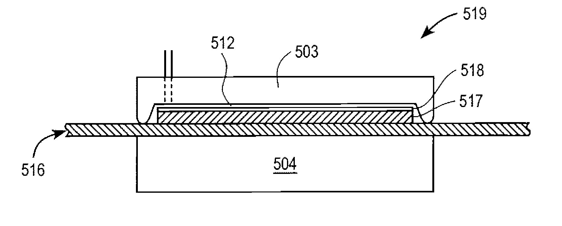
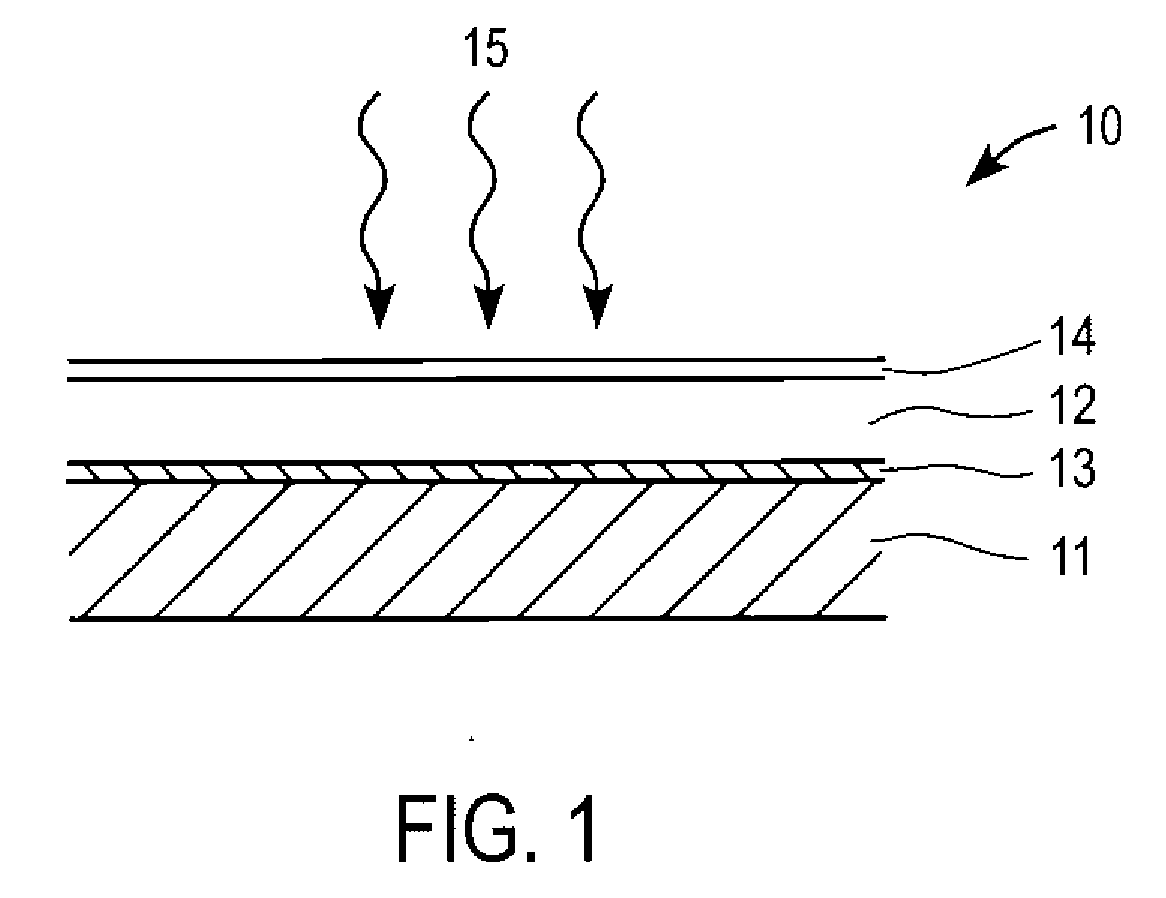
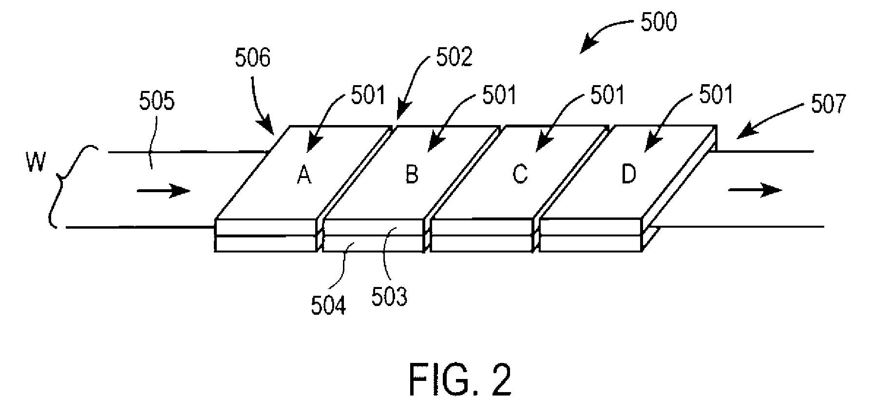
[0050] A Mo coated stainless steel or aluminum foil may be used as the base. A metallic precursor comprising Cu, In, and Ga may be deposited oil the base. Multi-chamber process unit 603 shown in FIG. 4 may be used for the formation of a Cu(In,Ga)(S,Se)2 layer on the base. The base comprising the metallic precursor layer is depicted in FIG. 4 as substrate 602. The process unit 603 has chambers or sections indicated by dotted lines and labeled as A, B, C, D and E. The process unit has a single top body 600 and a single bottom body 601. Within the top body 600 and the bottom body 601 there are independent heating means to independently change and control temperatures of the individual sections A, B, C, D and E. There are also independent gas lines 604 that may act as gas inlets or outlets for each section.

[0051] In this example, section A is used for Se deposition oil the metallic precursor. Section B is used for initial reaction at a temperature of 150-250° C. Section C is used for c...


PUM

PropertyMeasurementUnit
Lengthaaaaaaaaaa
Temperatureaaaaaaaaaa
Flexibilityaaaaaaaaaa

Abstract

The present invention relates to method and apparatus for preparing thin films of semiconductor films for radiation detector and photovoltaic applications. In one aspect, the present invention includes a series of chambers between the inlet and the outlet, with each chamber having a gap that allows a substrate to pass therethrough and which is temperature controlled, thereby allowing each chamber to maintain a different temperature, and the substrate to be annealed based upon a predetermined temperature profile by efficiently moving through the series of chambers. In another aspect, each of the chambers opens and closes, and creates a seal when in the closed position during which time annealing takes place within the gap of the chamber. In a further aspect, the present invention provides a method of forming a Group IBIIIAVIA compound layer on a surface of a flexible roll.

Description

CLAIM OF PRIORITY [0001] This application claims priority to U.S. Provisional Appln. Ser. No. 60 / 728,638 filed Oct. 19, 2005 entitled “Method and Apparatus for Converting Precursor Films Into Solar Cell Absorber Layers” and to U.S. Provisional Appln. Ser. No. 60 / 782,373 filed Mar. 14, 2006 entitled “Method and Apparatus for Converting Precursor Layers Into Photovoltaic Absorbers”, both of which are incorporated by reference herein in their entirety.FIELD OF THE INVENTION [0002] The present invention relates to method and apparatus for preparing thin films of semiconductor films for radiation detector and photovoltaic applications. BACKGROUND [0003] Solar cells are photovoltaic devices that convert sunlight directly into electrical power. The most common solar cell material is silicon, which is in the form of single or polycrystalline wafers. However, the cost of electricity generated using silicon-based solar cells is higher than the cost of electricity generated by the more traditi...

Claims


Application Information

Patent Timeline
IPC IPC(8): H01L21/00C23C16/00
CPCC23C16/305C23C16/54H01L31/0322H01L31/03928Y02E10/541C23C16/4586C23C16/52H01L21/67207H01L31/04Y02E10/50
Inventor BASOL, BULENT M.
Owner SOLOPOWER
Why Eureka
Try Eureka