Micro patch coating device and method

a technology of coating device and micro-patch, which is applied in the direction of liquid transferring device, superimposed coating process, liquid/solution decomposition chemical coating, etc., can solve the problems of high cost of equipment installation, low material utility rate, and low yield ra

Active Publication Date: 2010-11-02
NAT TAIWAN UNIV
View PDF4 Cites 0 Cited by
  • Summary
  • Abstract
  • Description
  • Claims
  • Application Information

AI Technical Summary

Benefits of technology

[0017]The coating method in the present invention overcomes the low material utility rate problem happened in spin coating and photolithography, and is applicable in coating larger dimension display panels. The present invention also solves the problems of low yield rate and low production efficiency in ink injection method, and it allows high degree of variation of the pattern which cannot be achieved by stamping. The method of the present invention lowers the manufacturing costs, improves the production efficiency, and is capable to be used for producing larger dimension display panels and sophisticated micro patch patterns for matching the future development.
[0018]Furthermore, the present invention provides higher material utility rate than that of photolithography that requires repeated exposure procedures. The present invention saves the processing time. In the coating method of the present invention, coating patterns are formed by varying the output ratio of the coating and auxiliary fluid and the relative movements between the coating die and the substrate. Besides, by directly coating the two-phase fluid to the substrate, the pattern is easily changed than that produced by stamping. Meanwhile, the method does not require of high precision injection as that as required in conventional ink injecting and enables higher yield rate in production.

Problems solved by technology

However, due to low material utility rate, the method has recently been phased out by other developments, such as extrusion spin coating (as disclosed in U.S. Pat. No. 6,191,053) and slot patch coating (as disclosed in U.S. Pat. No. 4,938,994).
The method is not only too complicated, but also demands the installation of expensive equipment.
Besides, because of the poor resistance of dyes against heat and light, the dyeing method is limited to apply for fabrication of small sized colorful LCD and conventional CRT.
The pigment dispersing method is complicated and requires expensive equipment and the operation is time-consuming, and it has low utility rate of coloring material and limited variation in pixel pattern, and therefore this method is not potential to meet the future demands for larger size and lower price display panel.
Hence, a number of operation parameters are involved, making it difficult to control the yield rate accurately.
The inclusion of an additional transparent conductive film set forth by this method is the most significant drawback, as it lowers the light permeability and resolution, and hence it limits the layout of the patterns which cannot be too elaborate.
To conclude, the conventional coating technology fails to define patterns directly at coating, and it relies, instead, on exposure to remove excessive materials.
Thus, it results in low material utility rate throughout the whole process, e.g. less than one third of the material, failing to satisfy the needs for mass production and at low costs.
Despite of the advantages of high material utility rate and low manufacturing cost, this method provides limited variation of patterns, making it difficult to change the arrangement of the arrays of pixels at liberty.
Besides, the traveling paths of droplets are susceptible to air flow disturbance, and it is likely that the ink droplets are injected accidentally to adjacent blocks and results in contamination.
Also, the moving rate of the ink injecting head module is limited to secure precise injection.
Because each of ink injecting heads is allowed to jet only one droplet at one time, the production efficiency is very low.
In order to solve this problem, the numbers of the ink injecting heads have to be increased (which inevitably increase the cost).

Method used


Image

  • Micro patch coating device and method
  • Micro patch coating device and method
  • Micro patch coating device and method

Examples


Embodiment Construction

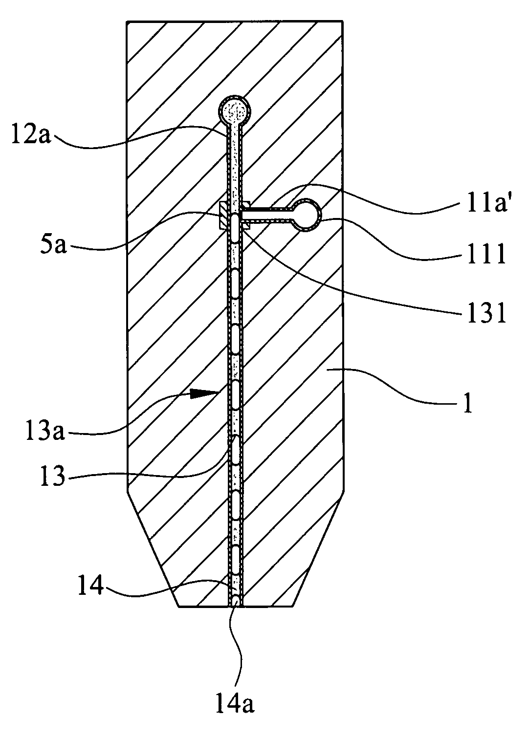
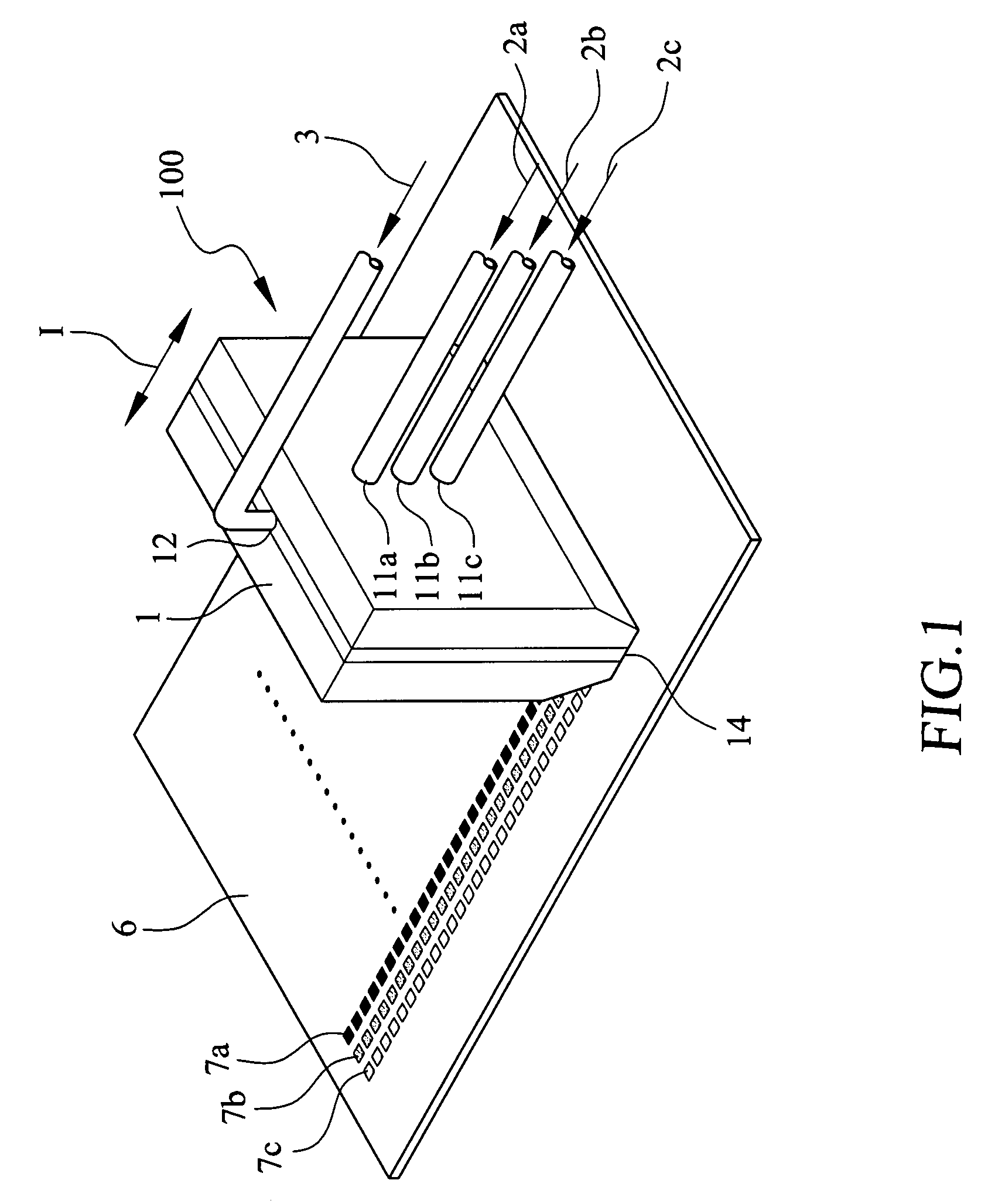
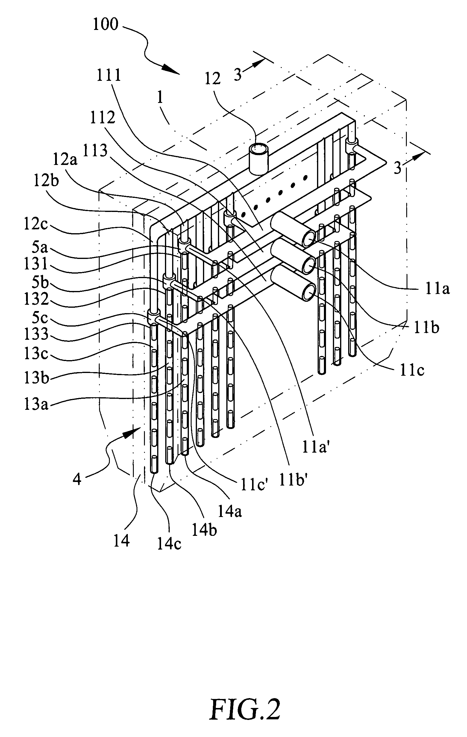
[0031]With reference to the drawings and in particular to FIGS. 1 to 3, a micro patch coating device 100 constructed in accordance with the present invention is shown, which comprises a coating die 1. The coating die 1 comprises a plurality of coating fluid inlets 11a, 11b, 11c and an auxiliary fluid inlet 12 arranged at specific positions. The coating fluid inlets 11a, 11b, 11c are used for respectively supplying coating fluids 2a, 2b, 2c into the coating die 1. Each of the coating fluids 2a, 2b, 2c contains a specific pigment, e.g. blue, green or red color pigment, which is different from each other and has specific composition. The auxiliary fluid inlet 12 is used for supplying an auxiliary fluid 3 to the coating die 1. The auxiliary fluid 3 may comprise a single fluid or a number of different fluids, based on the types of the coating fluids.

[0032]As shown in FIG. 2, the coating die 1 is provided with a micro channel structure 4 arranged at an interior of the coating die 1. The b...


PUM

PropertyMeasurementUnit
lengthaaaaaaaaaa
coloraaaaaaaaaa
colorsaaaaaaaaaa

Abstract

A micro patch coating device includes a coating die with a micro channel structure. A coating fluid is supplied through a coating fluid inlet and an auxiliary fluid is supplied through an auxiliary fluid inlet. After a segment of a predetermined length of the coating fluid is formed at a two-phase fluid output section, the coating fluid flow is intercepted. In turn, a segment of predetermined length of the auxiliary fluid is formed at the two-phase fluid output section, and then the auxiliary fluid flow is intercepted. A two-phase fluid is formed and flows out of the coating die to the substrate to form micro patches thereon.

Description

FIELD OF THE INVENTION[0001]The present invention relates to a coating device and method, and in particular to a micro patch coating device which can be applied in the fabrication of color filters of flat panel liquid crystal displays (LCD) and coloring unit of the fluorescent film in plasma display modules, or in the manufacturing of biomedical products and flexible electronics and cells.BACKGROUND OF THE INVENTION[0002]With the development of information technology, flat panel display has gradually replaced the conventional cathode ray tubes (CRT) display. Flat panel LCD, for instance, which takes up the largest market share among all flat panel displays, is composed of backlight source, light polarizer, glass substrate, liquid crystal, thin film transistor (TFT), color filter (CF), etc., while the color filter is the key component determining the color characteristics and contrast of a LCD.[0003]Color filters in LCD and coloring unit for the fluorescent film in plasma display pan...

Claims


Application Information

Patent Timeline
Patent Type & Authority Patents(United States)
IPC IPC(8): B05B7/08B67D7/52B05D5/00B05D1/26B05B7/06
CPCB41J3/407B05C5/0275B05C11/1034
Inventor WANG, AN-BANGLIN, I-CHUNWANG, YI-HUALEE, CHIH-KUNG
Owner NAT TAIWAN UNIV
Why Eureka
Try Eureka