Passivation layer etching method, manufacture method of pad and manufacture method of semiconductor device

A passivation layer, semiconductor technology, applied in the direction of semiconductor/solid-state device manufacturing, electrical components, circuits, etc., can solve problems such as the decline of etching rate, and achieve the effect of ensuring etching effect, solving the effect of reducing etching rate and ensuring performance

Inactive Publication Date: 2016-09-28
SHANGHAI HUAHONG GRACE SEMICON MFG CORP
View PDF5 Cites 7 Cited by
  • Summary
  • Abstract
  • Description
  • Claims
  • Application Information

AI Technical Summary

Problems solved by technology

[0007] The object of the present invention is to provide a passivation layer etching method and a manufacturing method of pads and semiconductor devices, which can solve the problem of etching rate decline and simultaneously obtain pads with better performance

Method used


Image

  • Passivation layer etching method, manufacture method of pad and manufacture method of semiconductor device
  • Passivation layer etching method, manufacture method of pad and manufacture method of semiconductor device
  • Passivation layer etching method, manufacture method of pad and manufacture method of semiconductor device

Examples


Embodiment Construction

[0034] In order to make the purpose and features of the present invention more obvious and understandable, the specific implementation of the present invention will be further described below in conjunction with the accompanying drawings. However, the present invention can be implemented in different forms and should not be limited to the described embodiments.

[0035] Please refer to image 3 , the invention provides a passivation layer etching method, comprising:

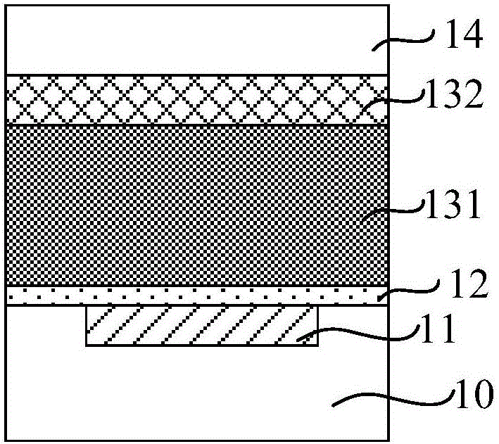
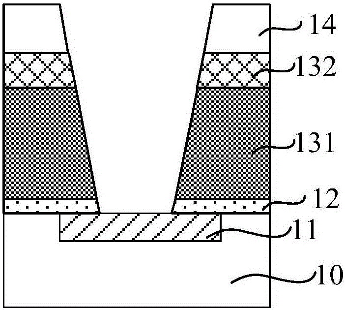
[0036] S1, sequentially forming an etch barrier layer, a first passivation layer and a second passivation layer on a semiconductor substrate with a top metal layer formed on the surface, the material of the first passivation layer and the second passivation layer are different and the thickness is greater than the second passivation layer;

[0037] S2, forming a patterned photoresist layer aligned with the top layer metal on the second passivation layer;

[0038] S3, using the patterned photoresist layer as a m...


PUM


Abstract

The invention provides a passivation layer etching method, a manufacture method of a pad and a manufacture method of a semiconductor device. A first etching gas of relatively high fluorocarbon content is used to etch a passivation layer structure, an etching polymer can be prevented from accumulating in an etching cavity or in the sidewall of the passivation layer effectively, and the etching effect of the passivation layer is ensured; and a second etching gas of relatively low fluorocarbon content is used to etch an etching barrier layer under the passivation layer structure, over etching time of the etching barrier layer can be shortened greatly, top-layer metal below is prevented from excessive etching, and etched top-layer metal is prevented from accumulation in the etching cavity. Thus, the problem that the etching speed is decreased is solved effectively, and performances of the pad and the semiconductor device are ensured.

Description

technical field [0001] The invention relates to the field of semiconductor manufacturing, in particular to a method for etching a passivation layer for solving the problem of reducing the etching rate of the passivation layer, and a method for manufacturing a pad and a semiconductor device. Background technique [0002] As the manufacture of integrated circuits develops towards Ultra Large-Scale Integration (ULSI: Ultra Large-Scale Integration), the circuit density on the chip is increasing, and the number of components on the chip is increasing, and the surface of the chip cannot provide enough area to Make the required interconnect structure (Interconnect). For this reason, a design method for multilayer interconnect structures with more than two layers is proposed. The design method forms grooves or through holes by etching the interlayer dielectric layer, and fills the grooves and through holes with conductive material to realize multi-layer electrical interconnection i...

Claims


Application Information

Patent Timeline
Patent Type & Authority Applications(China)
IPC IPC(8): H01L21/311H01L21/48
CPCH01L21/31116H01L21/31144H01L21/4814
Inventor 陈宏曹子贵王卉徐涛
Owner SHANGHAI HUAHONG GRACE SEMICON MFG CORP
Why Eureka
Try Eureka