Production process method of PCB

A production process and PCB board technology, applied in the field of PCB board production process, can solve the problems of high production cost and environmental pollution, and achieve the effect of increasing income, reducing production cost and improving working environment

Pending Publication Date: 2022-01-18
KUNSHAN DONGWEI MACHINERY CO LTD
View PDF0 Cites 0 Cited by
  • Summary
  • Abstract
  • Description
  • Claims
  • Application Information

AI Technical Summary

Problems solved by technology

[0006] Therefore, the technical problem to be solved by the present invention is to overcome the defects of environmental pollution and high production cost caused by copper-containing etching waste liquid produced in the PCB board production process in the prior art, thereby providing an environmentally friendly, economical, and streamlined PCB The production process of the board

Method used


Image

  • Production process method of PCB
  • Production process method of PCB

Examples


Embodiment 1

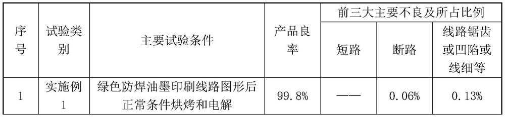
[0035] The present embodiment provides a kind of production technology method of PCB board, specifically comprises the following steps:

[0036] S1. Pre-printing treatment of the single panel: Use dilute sulfuric acid with a mass concentration of 5% to pickle the surface of the typesetting and cutting single panel, then wash it with water, and then use a 600-mesh nylon brush for grinding treatment, wash with water Finally, dry at 90°C;

[0037] S2. The side of the single-sided panel with copper foil is printed with solder resist ink to print the circuit pattern: use Guangxin green oil to print the circuit pattern on the surface of the pre-treated single-sided panel. The ink thickness of the circuit pattern is 15 μm, and then the circuit pattern is printed. Bake the single panel at 150°C for 30 minutes;

[0038] S3. Text printing on the other side of the single-sided board, that is, the substrate side: use white text ink to print text on the other side of the printed circuit g...

Embodiment 2

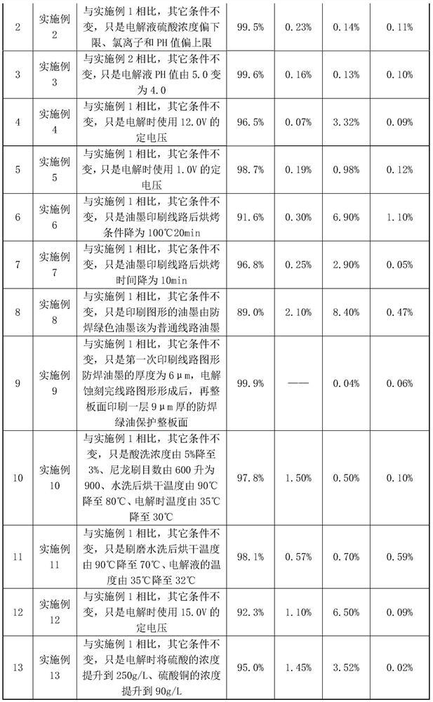
[0043] This embodiment provides a production process for PCB boards. The only difference from Embodiment 1 is that the concentration of sulfuric acid in the electrolyte used in the S4 step is 180g / L, the concentration of copper sulfate is 70g / L, and the concentration of chloride ions is 80ppm, and the pH of the electrolyte is 5.0.

[0044] The good product rate of the PCB board prepared by the method of this embodiment is 99.5%.

Embodiment 3

[0046] This embodiment provides a production process for PCB boards. The only difference from Embodiment 1 is that the concentration of sulfuric acid in the electrolyte used in the S4 step is 180g / L, the concentration of copper sulfate is 70g / L, and the concentration of chloride ions is 60ppm, and the pH of the electrolyte is 4.0.

[0047] The good product rate of the PCB board prepared by the method of this embodiment is 99.6%.


PUM


Abstract

The invention relates to the technical field of circuit board manufacturing, in particular to a production process method of a PCB, which comprises an etching method for forming a circuit pattern, and the etching method is electrolytic etching. According to the production process method of the PCB, chemical etching in a traditional PCB production process is replaced with electrolytic etching, the method is green, environmentally friendly and free of pollution, the production cost is greatly saved, the workshop operation environment is improved, and the strict acceptance standard of clean and civilized production is met.

Description

technical field [0001] The invention relates to the technical field of circuit board production, in particular to a production process method of a PCB board. Background technique [0002] The PCB board is a printed circuit board, and its single panel is generally a copper-clad substrate, which is a carrier for interconnection between electronic components. The PCB single-sided board is the most basic PCB board, and the parts are concentrated on one side, and the wires are concentrated on the other side of the PCB. There are many types of single-sided PCB boards on the market, which are suitable for various industries and fields, such as computers, digital products, medical equipment, aerospace, etc. [0003] The production process of a conventional single-sided PCB board includes: pre-processing the single-sided PCB board, and then directly printing the circuit pattern with circuit ink on the side with the copper layer. After the plate printing is pre-baked, it goes throug...

Claims


Application Information

Patent Timeline
Patent Type & Authority Applications(China)
IPC IPC(8): H05K3/00
CPCH05K3/00H05K3/002H05K3/0026
Inventor 刘建波朱爱明江泽军吴志鹏
Owner KUNSHAN DONGWEI MACHINERY CO LTD
Why Eureka
Try Eureka