

Semiconductor device and manufacturing method thereof
A manufacturing method and semiconductor technology, applied in semiconductor/solid-state device manufacturing, semiconductor devices, electric solid-state devices, etc., can solve the problems of rough p-type GaN layer, easy reduction of p-type GaN layer crystallinity, and difficulty in practical application
- Summary
- Abstract
- Description
- Claims
- Application Information
AI Technical Summary
Problems solved by technology
Method used
Image

Examples
no. 1 Embodiment approach
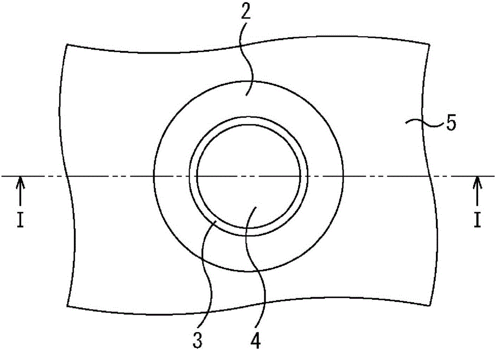
[0093] First, the first embodiment will be described. Figure 1A It is a plan view showing the structure of the semiconductor device (Schottky barrier diode) according to the first embodiment, Figure 1B is along Figure 1A A cross-sectional view of the I-I line in .
[0094] In the first embodiment, if Figure 1A and Figure 1B As shown, an AlN nucleation layer 1a is formed on a sapphire substrate 1, and an n-type GaN layer 2 is formed on the AlN nucleation layer 1a. The surface of the n-type GaN layer 2 on the AlN nucleation layer 1a is a Ga plane ((0001) plane in terms of Miller index). A ring-shaped InGaN layer 3 is formed on the n-type GaN layer 2 as a guard ring. Furthermore, an anode electrode (Schottky electrode) 4 forming a Schottky junction with the n-type GaN layer 2 is formed inside the InGaN layer 3 . Anode electrode 4 is thicker than InGaN layer 3 , and the outer peripheral portion of anode electrode 4 is in contact with the upper surface of InGaN layer 3 . I...
no. 2 Embodiment approach
[0121] Next, a second embodiment will be described. Figure 5 It is a cross-sectional view showing the structure of the semiconductor device (Schottky barrier diode) according to the second embodiment.
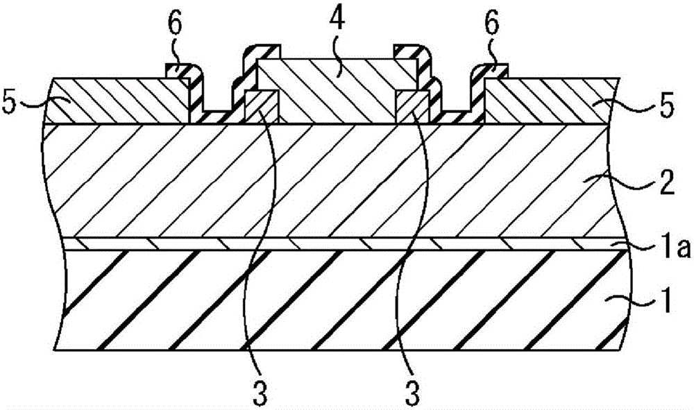
[0122] In the second embodiment, if Figure 5 As shown, the n-type impurity doped with n-type impurities at a concentration higher than that of the n-type GaN layer 2 is formed on the AlN nucleation layer 1a. + GaN layer 7 . Also, the n-type GaN layer 2 is only directly below the InGaN layer 3 and the anode electrode 4, and between the InGaN layer 3 and the anode electrode 4 and the n-type + Formed between the GaN layer 7, the cathode electrode 5 is not connected to the n-type GaN layer 2 but to the n + GaN layer 7 forms an ohmic junction. Other configurations are the same as those of the first embodiment.
[0123] The same effect as that of the first embodiment can be obtained also in the Schottky barrier diode with such a mesa structure. In addition, due to the high co...
no. 3 Embodiment approach
[0125] Next, a third embodiment will be described. Figure 6 It is a cross-sectional view showing the structure of the semiconductor device (Schottky barrier diode) according to the third embodiment.
[0126] In the third embodiment, a conductive n-type GaN substrate 1 b is used instead of the sapphire substrate 1 . and, if Figure 6 As shown, instead of the cathode electrode 5 being formed on the n-type GaN layer 2, the cathode electrode 21 is formed on the back surface of the n-type GaN substrate 1b. Other configurations are the same as those of the first embodiment.
[0127] The same effect as that of the first embodiment can be obtained also in the Schottky barrier diode having such a vertical structure. In addition, area can be saved. In addition, since the cathode electrode 21 can be formed regardless of the position of the anode electrode 4 and the like, the manufacturing process can also be simplified.
PUM
 Abstract
Description
Claims
Application Information