
Copper/ceramic bond and power module substrate

A technology of power modules and joints, which is applied in the manufacture of electric solid state devices, semiconductor devices, semiconductor/solid state devices, etc., and can solve problems such as cracking of ceramic substrates

Active Publication Date: 2016-09-28
MITSUBISHI MATERIALS CORP
View PDF7 Cites 14 Cited by
  • Summary
  • Abstract
  • Description
  • Claims
  • Application Information

AI Technical Summary

Problems solved by technology

Since the Ti oxide layer is hard and brittle, the ceramic substrate may be cracked under thermal cycle load

Method used


Image

  • Copper/ceramic bond and power module substrate
  • Copper/ceramic bond and power module substrate
  • Copper/ceramic bond and power module substrate

Examples


no. 1 approach

[0051] Hereinafter, a first embodiment according to a first aspect of the present invention will be described with reference to the drawings.

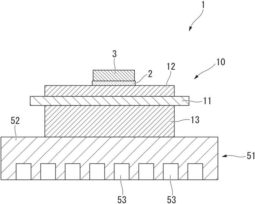
[0052] The copper-ceramic bonded body according to the first embodiment of the present invention is formed by joining the ceramic substrate 11 which is a ceramic part made of nitride ceramics and the copper plate 22 which is a copper part made of copper or a copper alloy (circuit The power module substrate 10 constituted by layer 12).

[0053] figure 1 A power module substrate 10 according to the first embodiment of the present invention and a power module 1 using the power module substrate 10 are shown in FIG.

[0054] The power module 1 includes a power module substrate 10, and is bonded to one side of the power module substrate 10 via a solder layer 2 ( figure 1 The semiconductor element 3 on the upper side) and the other side of the power module substrate 10 ( figure 1 The lower side of the middle) radiator 51.

[0055] Here, t...

no. 2 approach

[0092] Hereinafter, a second embodiment according to the first aspect of the present invention will be described with reference to the drawings.

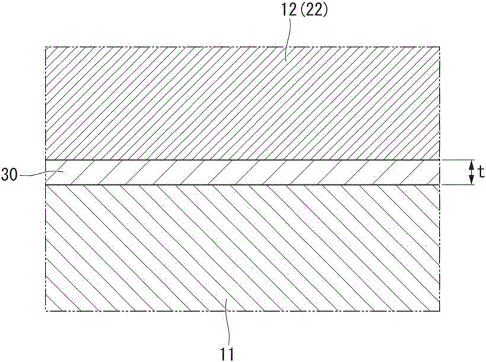
[0093] The copper-ceramic bonded body according to the second embodiment of the present invention is configured by bonding the ceramic substrate 11 which is a ceramic component made of nitride ceramics and the ceramic substrate 11 made of copper or a copper alloy, as in the first embodiment. A power module substrate composed of a copper plate 22 (circuit layer 12) of copper components, figure 1 In the power module substrate shown, the structure of the bonding interface between the ceramic substrate 11 and the copper plate 22 (circuit layer 12 ) is different.

[0094] Figure 5 The structure of the bonding interface between the ceramic substrate 11 and the copper plate 22 (circuit layer 12 ) in the second embodiment of the present invention is shown in .

[0095] In the second embodiment, as Figure 5 As shown, the bonding interfa...

no. 3 approach

[0127] Hereinafter, a third embodiment according to the second aspect of the present invention will be described with reference to the drawings.

[0128] Components having the same configuration as those of the first embodiment are assigned the same reference numerals, and detailed description thereof will be omitted.

[0129] The copper-ceramic bonded body according to the third embodiment is formed by bonding a ceramic substrate 211 which is a ceramic member made of alumina and a copper plate 22 (circuit layer 12 ) which is a copper member made of copper or a copper alloy. A power module substrate 210 is formed.

[0130] Figure 8 A power module substrate 210 as a third embodiment of the present invention and a power module 201 using the power module substrate 210 are shown in FIG.

[0131] The power module 201 includes a power module substrate 210, and is bonded to one side of the power module substrate 210 via a solder layer 2 ( Figure 8 The semiconductor element 3 on ...


PUM

PropertyMeasurementUnit
thicknessaaaaaaaaaa
thicknessaaaaaaaaaa
thicknessaaaaaaaaaa

Abstract

The invention discloses a copper / ceramic bond and a power module substrate. The copper / ceramic bond formed by bonding a copper member (22) comprising copper or copper alloy to a ceramic member (11) comprising nitride ceramic, wherein in a bonded interface of the copper member (22) and ceramic member (11) an active element oxide layer (30) containing an active element and oxygen is formed, and the active element oxide layer (30) has a thickness (t) in the range of 5 to 220 nm.

Description

technical field [0001] The present invention relates to a copper-ceramic bonded body formed by bonding a copper component made of copper or a copper alloy and a ceramic component, and a substrate for a power module composed of the copper-ceramic bonded body. [0002] This application claim is based on the patent application No. 2014-024410 filed in Japan on February 12, 2014, the patent application No. 2014-052594 filed in Japan on March 14, 2014, and the patent application filed in Japan on July 2, 2014 Priority of No. 2014-136567, the contents of which are incorporated herein. Background technique [0003] In a semiconductor device such as an LED or a power module, a semiconductor element is bonded to a circuit layer made of a conductive material. [0004] Power semiconductor elements for high-power control used to control wind power generation, electric vehicles, hybrid vehicles, etc., have a large amount of heat generation, so as the substrate on which the element is mo...

Claims


Application Information

Patent Timeline
Patent Type & Authority Applications(China)
IPC IPC(8): C04B37/02H01L23/12H01L23/13H01L23/36
CPCC04B37/025C04B37/026H01L23/15H01L23/3735H01L23/473C04B2235/6581C04B2235/72C04B2237/068C04B2237/121C04B2237/126C04B2237/343C04B2237/366C04B2237/368C04B2237/407C04B2237/60C04B2237/704C04B2237/706C04B2237/708H01L2224/32225C04B2237/38H01L24/29H01L2224/29111H01L24/32H01L2924/01047H01L2924/01049H01L2924/01029C04B37/003C04B37/023C04B2237/06C04B2237/124C04B2237/345C04B2237/346H01L21/4807H01L21/4871H01L23/142H01L2224/32505H01L2924/0105H01L2924/01079H01L2924/014H05K1/09
Inventor 寺崎伸幸长友义幸
Owner MITSUBISHI MATERIALS CORP
Learn More