Semiconductor element mounting method and mounting substrate

An installation method and semiconductor technology, applied in semiconductor/solid-state device components, semiconductor devices, semiconductor/solid-state device manufacturing, etc., can solve problems such as inability to install, time required, pollution, etc., and achieve the effect of easy deformation

Inactive Publication Date: 2005-04-13
PANASONIC CORP
View PDF2 Cites 5 Cited by
  • Summary
  • Abstract
  • Description
  • Claims
  • Application Information

AI Technical Summary

Problems solved by technology

However, in this method of reflow mounting of solder bumps, in order to melt the solder bumps, for example, each solder bump needs to be heated to 238°C or higher. However, since the allowable temperature of the LED is below 200°C, this reflow mounting cannot be used. Method for LED installation
Moreover, when the reflow occurs, the light-emitting surface of the LED is polluted by the gas components in the reflow atmosphere, and there is also a problem that the light-emitting function is reduced.
[0019] And even when the semiconductor element is not an LED, assuming that the above-mentioned allowable temperature is 238°C or higher, a flux supply process and a cleaning process are required along with the use of solder, and this reflow mounting method also requires time and manpower.

Method used


Image

  • Semiconductor element mounting method and mounting substrate
  • Semiconductor element mounting method and mounting substrate
  • Semiconductor element mounting method and mounting substrate

Examples


Embodiment Construction

[0089] Before continuing to describe the present invention, the same reference numerals are given to the same components in the drawings.

[0090] Embodiments according to the present invention will be described in detail below based on the drawings.

[0091] (first implementation)

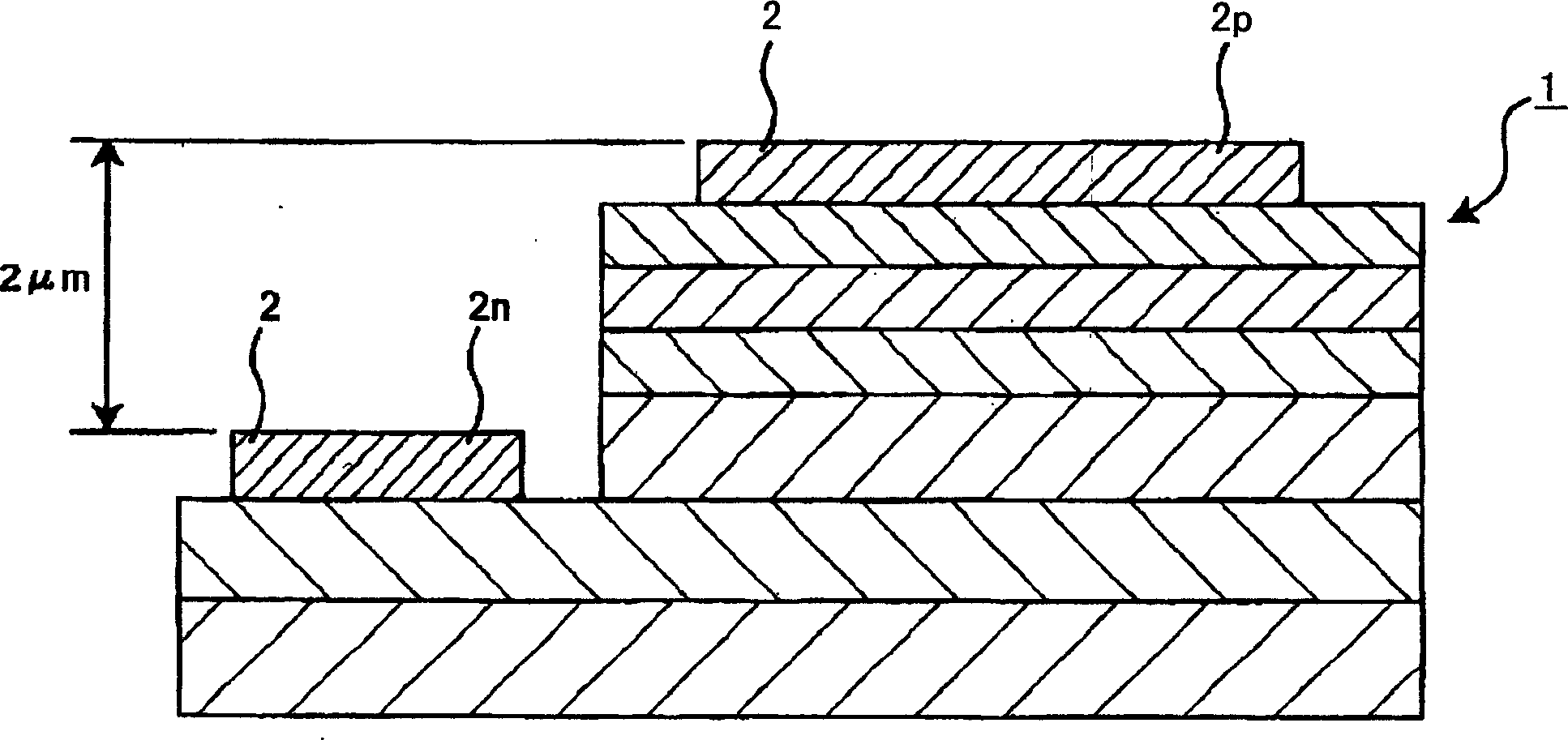
[0092] In the semiconductor element mounting method according to the first embodiment of the present invention, as an example of the above-mentioned semiconductor element, in figure 1 A schematic illustration of a planar structure in which LED chips (or LED elements) are mounted on a substrate is shown in .

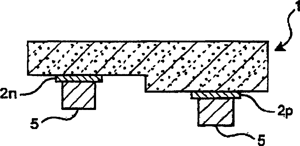
[0093] Such as figure 1 As shown, an LED (Light Emitting Diode: Light Emitting Diode) chip 1 has a substantially square shape, and a plurality of pads 2 serving as an example of element electrodes are formed on the surface on the bonding side with a substrate. Each pad 2 can be divided into two types according to the characteristics of the LED chip 1: one is to form an oblong P pole pad ...


PUM


Abstract

The bonding member formed by the gold nano paste is arranged between the above-mentioned each element electrode and the above-mentioned each substrate electrode, and the above-mentioned each element electrode is connected to the above-mentioned each substrate electrode by means of the above-mentioned each bonding member. Each bonding member imparts ultrasonic vibrations to bond the respective bonding members to the respective substrate electrodes and the respective element electrodes.

Description

technical field [0001] The present invention relates to a semiconductor element mounting method and a semiconductor element mounting substrate for producing a semiconductor element mounting substrate by mounting the semiconductor element on the substrate while bonding a substrate electrode of the substrate to an element electrode of the semiconductor element. Background technique [0002] In the past, an LED (LED element), which is an example of such a semiconductor element, has been used in applications such as fluorescent lamps by taking advantage of its light-emitting performance. However, although LEDs can be made to emit light by applying a voltage, heat is generated along with the light emission, and the luminous efficiency of the LED decreases due to the heat generation, resulting in a problem of low luminance. In order to solve this problem, various methods have been conceived in the past for effectively avoiding the heat generated in LEDs. [0003] For example, as ...

Claims


Application Information

Patent Timeline
Patent Type & Authority Applications(China)
IPC IPC(8): H01L21/607H01L23/485H01L23/498H01L33/62
CPCH01L23/49811H01L24/81H01L33/62H01L2224/0401H01L2224/0603H01L2224/1131H01L2224/1134H01L2224/1308H01L2224/13082H01L2224/13144H01L2224/13644H01L2224/1403H01L2224/16H01L2224/81192H01L2224/81194H01L2224/81205H01L2224/81801H01L2224/85424H01L2924/01004H01L2924/01013H01L2924/01015H01L2924/01033H01L2924/01078H01L2924/01079H01L2924/01082H01L2924/09701H01L24/75H01L2924/00013H01L2924/01006H01L2924/01023H01L2924/01047H01L2924/0105H01L2924/014H01L2924/12041H01L2224/16225H01L2224/32225H01L2224/73204H01L2224/92125H01L2924/10253H01L2224/06102H01L24/06H01L24/13H01L24/14H01L24/16H01L2224/11505H01L2924/00014H01L2224/13099H01L2924/00
Inventor 内藤浩幸仕田智土师宏森川诚
Owner PANASONIC CORP
Why Eureka
Try Eureka