

Desoldering method of semiconductor device
A technology of components and semiconductors, which is applied in the field of desoldering of semiconductor components, can solve the problems of easy damage to the device body and complicated operation, and achieve the effect of improving the yield rate and processing efficiency, high safety, and the safety of the desoldering and separation process
- Summary
- Abstract
- Description
- Claims
- Application Information
AI Technical Summary
Problems solved by technology
Method used
Image

Examples
Embodiment 1
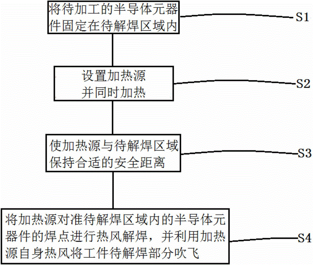
[0023] Such as figure 1 As shown, a method for desoldering semiconductor components, the method for desoldering semiconductor components includes the following steps:
[0024] Step S1: fixing the semiconductor components to be processed in the area to be desoldered;
[0025] Fix the semiconductor components in the area to be desoldered by bolts.
[0026] Step S2: setting the heating source and heating at the same time;
[0027] The step S2: setting a heating source near the area to be desoldered and simultaneously heating includes: the heating time is between 50s and 60s, and the temperature is between 700°C and 800°C.
[0028] The heating source is mainly a heat gun, which uses the principle of hot air to directly blow and fill the solder joints of the part to be removed on the semiconductor component to melt the solder around it, and then use the heat of the heat gun to blow away the part to be removed. Moreover, the distance between the heat gun and the semiconductor com...
Embodiment 2
[0038] Such as figure 1 As shown, a method for desoldering semiconductor components, the method for desoldering semiconductor components includes the following steps:
[0039] Step S1: fixing the semiconductor components to be processed in the area to be desoldered;
[0040] Fix the semiconductor components in the area to be desoldered by bolts.
[0041] Step S2: setting the heating source and heating at the same time;
[0042] The step S2: setting the heating source and simultaneously heating includes: the heating time is between 50s and 60s, and the temperature is between 700°C and 800°C.
[0043] The heating source is mainly a heat gun, which uses the principle of hot air to directly blow and fill the solder joints of the part to be removed on the semiconductor component to melt the solder around it, and then use the heat of the heat gun to blow away the part to be removed. Moreover, the distance between the heat gun and the semiconductor components and the temperature o...
Embodiment 3
[0053] Such as figure 1 As shown, a method for desoldering semiconductor components, the method for desoldering semiconductor components includes the following steps:
[0054] Step S1: fixing the semiconductor components to be processed in the area to be desoldered;
[0055] Fix the semiconductor components in the area to be desoldered by bolts.
[0056] Step S2: setting the heating source and heating at the same time;
[0057] The step S2: setting the heating source and simultaneously heating includes: the heating time is between 50s and 60s, and the temperature is between 700°C and 800°C.
[0058] The heating source is mainly a heat gun, which uses the principle of hot air to directly blow and fill the solder joints of the part to be removed on the semiconductor component to melt the solder around it, and then use the heat of the heat gun to blow away the part to be removed. Moreover, the distance between the heat gun and the semiconductor components and the temperature o...
PUM
 Abstract
Description
Claims
Application Information