Gap fill treatment for via process

A technology of manufacturing process and processing method, which is applied in the direction of semiconductor/solid-state device manufacturing, electrical components, circuits, etc., and can solve the unevenness of the surface of the gap filling material layer thickness difference, the solvent erosion of the trench filling material layer, and the inability to deal with uneven thickness, etc. problem, to achieve the effect of preventing solvent erosion, eliminating step height difference, and avoiding defocusing

Inactive Publication Date: 2016-10-05
POWERCHIP TECH CORP
View PDF3 Cites 0 Cited by
  • Summary
  • Abstract
  • Description
  • Claims
  • Application Information

AI Technical Summary

Problems solved by technology

However, the existing etch-back method cannot deal with the uneven thickness of the trench filling material layer of each opening (that is, the step height difference) caused by the pattern density.
In addition, for the existing etch-back method, there is also the problem that the trench filling material layer is easily eroded by the solvent in the subsequent manufacturing process, so that the thickness difference of the trench filling material layer filled in the opening and the unevenness of the pattern surface cannot be solved. solved

Method used


Image

  • Gap fill treatment for via process
  • Gap fill treatment for via process
  • Gap fill treatment for via process

Examples


Embodiment Construction

[0038] Embodiments of the invention are described more fully hereinafter with reference to the accompanying drawings. However, the present invention may be practiced in many different forms and is not limited to the embodiments set forth herein. The directional terms mentioned in the following embodiments, such as "upper", etc., are only referring to the directions of the attached drawings, so the directional terms used are for explaining the description rather than limiting the present invention. In addition, the size and relative size of each layer may be exaggerated for the sake of clarity in the drawings.

[0039] Hereinafter, a trench filling method for a via manufacturing process according to an embodiment of the present invention will be described.

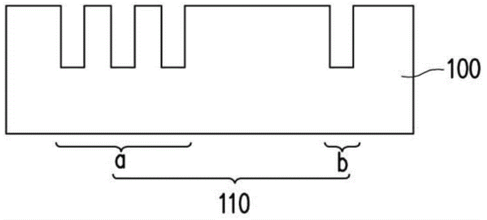
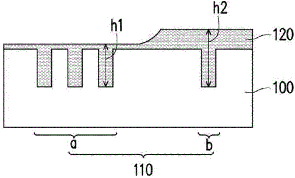
[0040] First, please refer to Figure 1A , providing a substrate 100. The substrate 100 is, for example, a silicon substrate or a semiconductor structure covered with a dielectric layer, a semiconductor material layer, o...


PUM


Abstract

A gap fill treatment for via process is provided. A substrate with a plurality of openings has formed therein is provided. The substrate includes a dense pattern region and an isolated pattern region. A positive resist layer is formed to fill in the openings on the substrate, wherein the thickness of the positive resist layer on the surface of the isolated pattern region is greater than that on the surface of the dense pattern region. The positive resist layer on the surface of the substrate is exposed only. The exposed positive resist layer is developed to form a gap-filling material layer, wherein the gap-filling material layer has the same thickness in the dense pattern region and in the isolated pattern region. A reagent is coated on the surface to form a reaction layer. The reaction layer is removed so that a cap layer remained on the gap-filling material layer.

Description

technical field [0001] The invention relates to a manufacturing process of a semiconductor element, and in particular to a trench filling treatment method for the manufacturing process of a via window. Background technique [0002] Today, with the vigorous development of integrated circuits, the miniaturization and integration of components is an inevitable trend, and it is also an important topic for the industry to actively develop. The key to the device size in the entire semiconductor manufacturing process lies in the technology of the photolithography manufacturing process. Moreover, with the high integration of semiconductor devices, the critical dimension (CD) of integrated circuits is getting smaller and smaller, so the resolution required by the photolithography manufacturing process is getting higher and higher. [0003] Wherein, during the semiconductor manufacturing process, it is often necessary to perform gap fill treatment on various openings. The openings f...

Claims


Application Information

Patent Timeline
Patent Type & Authority Applications(China)
IPC IPC(8): H01L21/762H01L21/768
CPCH01L21/31058H01L21/76808H01L21/31144
Inventor 林晓江林冠亨
Owner POWERCHIP TECH CORP
Why Eureka
Try Eureka