
Photosensitive module and manufacturing method thereof

A photosensitive module and module technology, applied in the photosensitive field, can solve the problem that the thinness of electronic photosensitive imaging products cannot be further improved, and achieve the effects of reducing the probability of impurities contaminating the image sensor, reducing the failure rate, and reducing the thickness

Active Publication Date: 2019-07-26
LENOVO (BEIJING) LTD
View PDF8 Cites 0 Cited by
  • Summary
  • Abstract
  • Description
  • Claims
  • Application Information

AI Technical Summary

Problems solved by technology

[0007] This application provides a photosensitive module and a manufacturing method to solve the problem in the prior art that the thinness of electronic photosensitive imaging products cannot be further improved while ensuring a certain imaging quality

Method used


Image

  • Photosensitive module and manufacturing method thereof
  • Photosensitive module and manufacturing method thereof
  • Photosensitive module and manufacturing method thereof

Examples


Embodiment 1

[0060] Please refer to figure 2 , Embodiment 1 of the present application provides a photosensitive module, including:

[0061] A printed circuit board 22, including a receiving part 221;

[0062] An image sensor 23, the image sensor is at least partially housed in the housing part, so that the distance between the printed circuit board and the packaging component is smaller than the thickness of the image sensor;

[0063] The packaging component is connected with the printed circuit board and used for packaging the image sensor.

[0064] Since the receiving part is provided on the printed circuit board, and the image sensor is at least partially housed in the receiving part, when the photosensitive module in the embodiment of the present application is placed horizontally and the glass cover is located above the printed circuit board, The image sensor is at a position slightly lower than the printed circuit board relative to the glass cover. It can be seen that the technic...

Embodiment 2

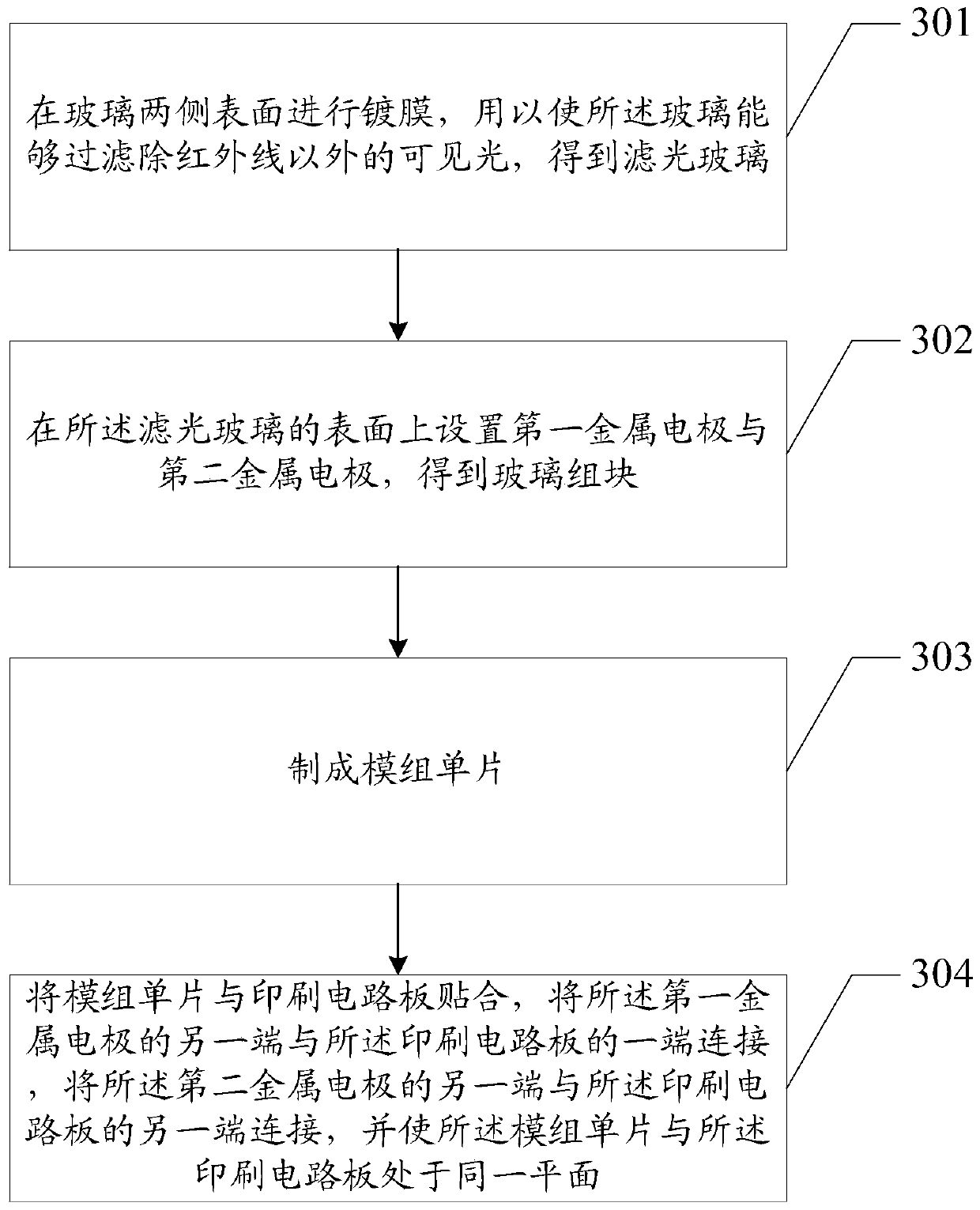
[0081] Please refer to image 3 , Embodiment 2 of the present application provides a method for manufacturing the photosensitive module as claimed in claim 1, comprising:

[0082] Step 301: coating the surfaces of both sides of the glass to enable the glass to filter visible light except infrared rays to obtain filter glass;

[0083]Step 302: setting a first metal electrode and a second metal electrode on the surface of the filter glass to obtain a glass cover;

[0084] Step 303: attach the image sensor to the glass cover, make the first metal electrode and the second metal electrode between the image sensor and the glass cover, and place the first metal The first end of the electrode is connected to the first end of the image sensor, the first end of the second metal electrode is connected to the second end of the image sensor, and the glass cover plate is cut according to predetermined specifications into modular monolithic pieces; or,

[0085] cutting the glass cover acc...


PUM


Abstract

The invention discloses a photosensitive module group and a manufacturing method thereof. A PCB is provided with an accommodating part, and at least part of an image sensor is accommodated in the accommodating part, so that the distance between the PCB and a packaging assembly is lower than the thickness of the image sensor. According to technical schemes of the invention, at least part of material of the PCB is left for the image sensor, raw materials is saved, and the distance between the PCB and the packaging assembly is lower than the thickness of the image sensor; and thus, the distance, which at least equals the thickness of the image sensor in the prior art, between the packaging assembly and the PCB is further decreased, the thickness of the photosensitive module group can be further decreased, and more raw material is saved.

Description

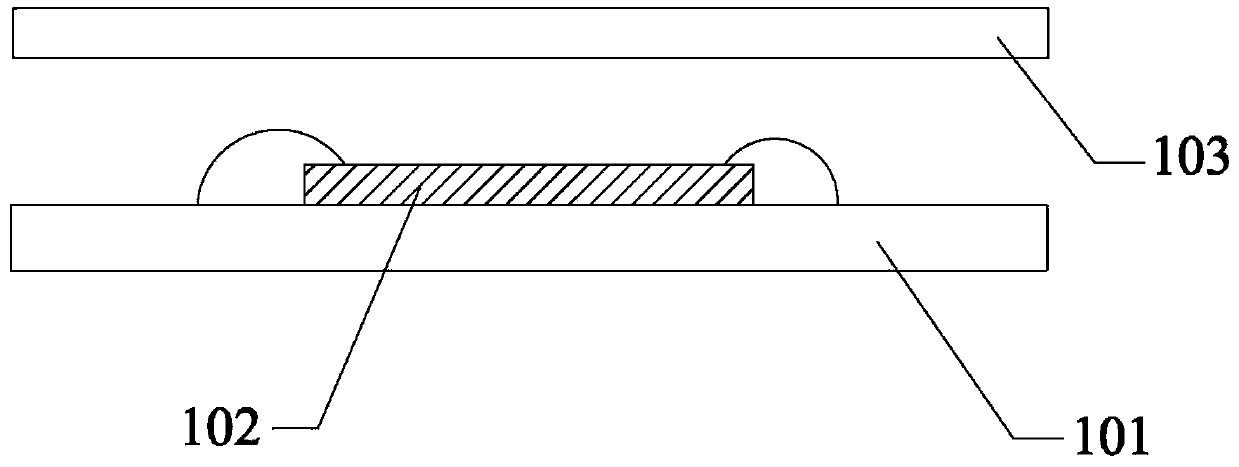
technical field [0001] The invention relates to the photosensitive field, in particular to a photosensitive module and a manufacturing method. Background technique [0002] At present, with the development of electronic technology, the appearance of existing electronic products is becoming thinner and thinner, and various functional applications are becoming more powerful. [0003] However, for existing electronic photosensitive imaging devices such as cameras and video cameras, if the thickness of the product is to be further reduced under the condition of thin and portable appearance design, it is necessary to reduce the thickness of each module inside the product, and each module inside the product includes Two parts, one part is the imaging module, and the other part is other components except the imaging module. [0004] Such as figure 1 As shown, in the existing electronic photosensitive imaging equipment, the imaging module generally has the following structure: the...

Claims


Application Information

Patent Timeline
Patent Type & Authority Patents(China)
IPC IPC(8): H01L27/146H01L21/82
Inventor 于宙刘杰王智虎
Owner LENOVO (BEIJING) LTD
Learn More