A full wave extraction method for differential through silicon via distribution parameters

An extraction method and a technology for distributing parameters, applied in the field of communications, can solve problems such as large errors and difficult to consider complex electromagnetic effects.

Inactive Publication Date: 2016-10-12
XIDIAN UNIV
View PDF0 Cites 7 Cited by
  • Summary
  • Abstract
  • Description
  • Claims
  • Application Information

AI Technical Summary

Problems solved by technology

The existing methods for extracting differential TSV distribution parameters all use theoretical model calculations, that is, analytical calculations or num

Method used


Image

  • A full wave extraction method for differential through silicon via distribution parameters
  • A full wave extraction method for differential through silicon via distribution parameters
  • A full wave extraction method for differential through silicon via distribution parameters

Examples


Embodiment Construction

[0080] Specific embodiments of the present invention will be described in detail below.

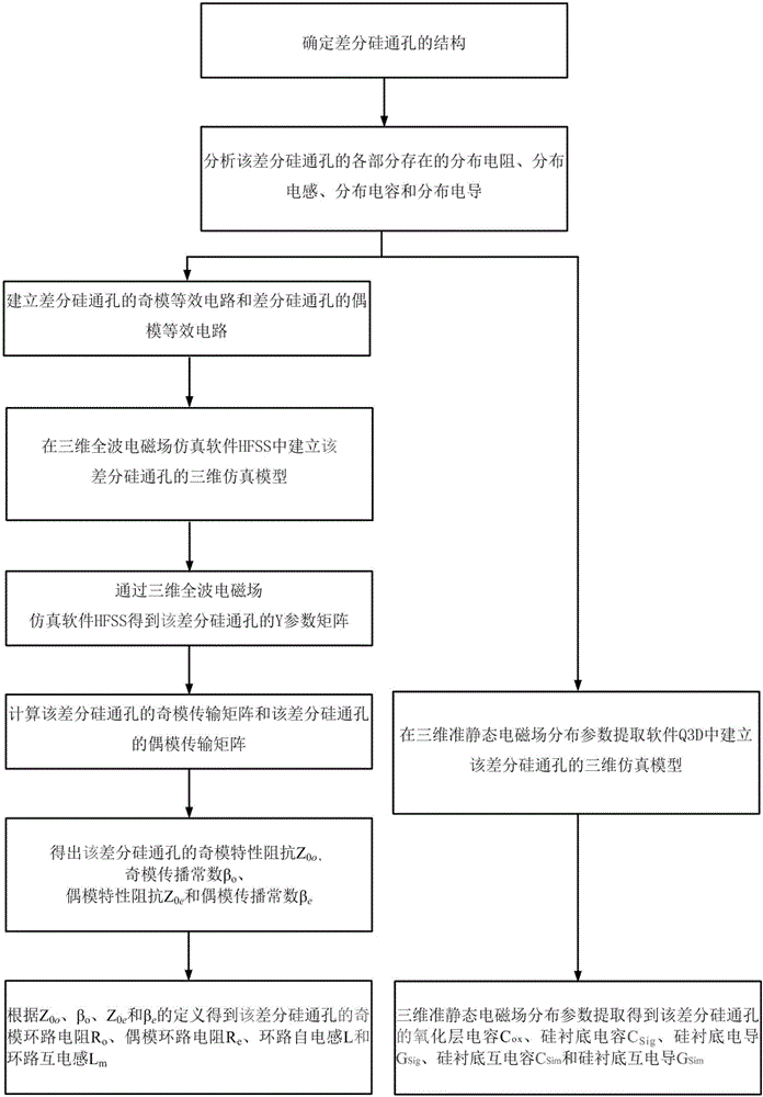
[0081] Such as figure 1 As shown, a full-wave extraction method of differential TSV distribution parameters includes the following steps:

[0082] 1) Determine the structure of the differential TSV;

[0083] 2), analyzing the distributed resistance, distributed inductance, distributed capacitance and distributed conductance existing in each part of the differential TSV;

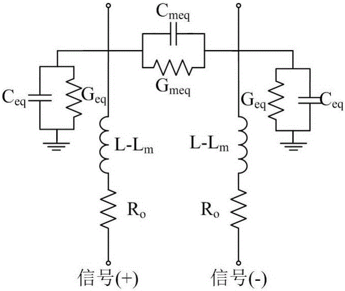
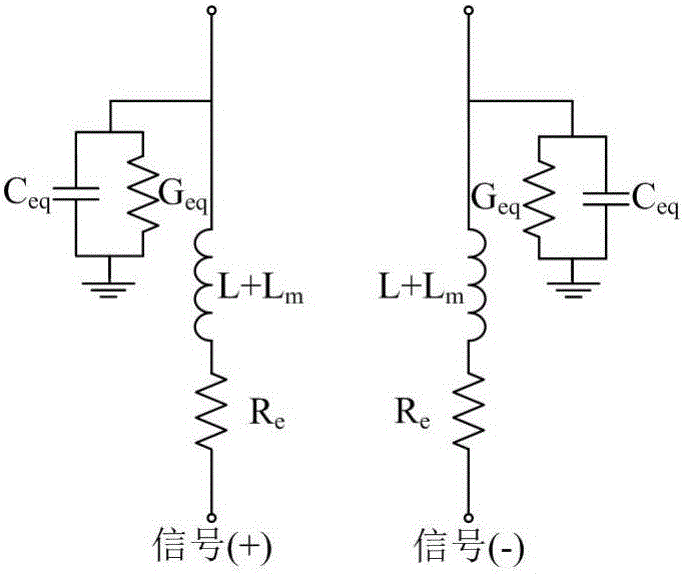
[0084] 3), establishing the odd-mode equivalent circuit of the differential TSV and the even-mode equivalent circuit of the differential TSV;

[0085] 4), establishing the three-dimensional simulation model of the differential TSV in the three-dimensional full-wave electromagnetic field simulation software HFSS;

[0086] 5), obtain the Y parameter matrix of the differential TSV through the three-dimensional full-wave electromagnetic field simulation software HFSS;

[0087] 6) Calculate the odd-mode transmission matri...


PUM


Abstract

The invention relates to a full wave extraction method for differential through silicon via distribution parameters. The method comprises the steps of determining a differential through silicon via structure; analyzing the distribution resistance, distribution inductance, distribution capacitance and distribution conductance of each part of the differential through silicon via; establishing an odd mode equivalent circuit and an even mode equivalent circuit of the differential through silicon via; establishing a differential through silicon via three-dimensional simulation model in HFSS; obtaining a Y-parameter matrix of the differential through silicon via and calculating an odd mode transmission matrix of the differential through silicon via and an even mode transmission matrix of the differential through silicon via; calculating the odd mode characteristic impedance Z0o and the odd mode propagation constant betao of the differential through silicon via; calculating the even mode characteristic impedance Z0e and the even mode propagation constant betae of the differential through silicon via; acquiring the odd mode loop resistance Ro, the even mode loop resistance Re, the loop self-inductance L and the loop mutual-inductance Lm of the differential through silicon via; establishing a three-dimensional simulation model of the differential through silicon via in Q3D and acquiring Cox, CSig, GSig, CSim and GSim.

Description

technical field [0001] The invention belongs to the communication field, and in particular relates to a full-wave extraction method of differential through-silicon hole distribution parameters. Background technique [0002] Three-dimensional integrated circuits (3D IC) have the advantages of high packaging density, strong noise immunity, low power loss, high operating speed and easy heterogeneous integration between different processes (logic, memory, radio frequency, analog, etc.), and can overcome Physical, process, and electrical constraints faced by many traditional planar integrated circuits. In a three-dimensional integrated circuit, a large number of homogeneous or heterogeneous chips are stacked, and through-silicon vias (TSVs) are used as vertical conductive channels between chips. These TSVs have become key components affecting the overall performance of 3D integrated circuits. [0003] According to the signal transmission mode, TSVs can be divided into single-en...

Claims


Application Information

Patent Timeline
IPC IPC(8): G06F17/50
CPCG06F30/23G06F30/367G06F30/398
Inventor 卢启军朱樟明丁瑞雪李跃进杨银堂
Owner XIDIAN UNIV
Why Eureka
Try Eureka