

Organic light emitting diode touch control display panel
A touch display panel, light-emitting diode technology, applied in static indicators, instruments, electrical digital data processing, etc., can solve the problems of poor display effect of OLED display panel, improve display effect, reduce process cost, realize thin the effect of
- Summary
- Abstract
- Description
- Claims
- Application Information
AI Technical Summary
Problems solved by technology
Method used
Image

Examples
Embodiment approach
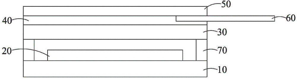
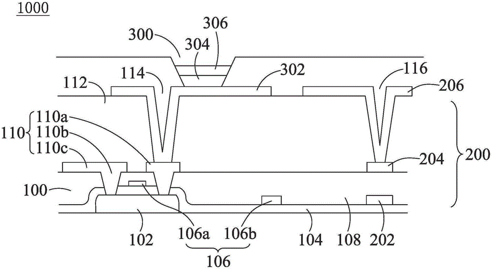
[0049] According to one embodiment, as Figure 4 As shown, the OLED bottom electrode 302 includes a bottom transparent conductive layer 302a, a top transparent conductive layer 302c, and a reflective layer 302b located between the bottom transparent conductive layer 302a and the top transparent conductive layer 302c. The touch sensing electrodes 206 can be located on the same layer as the bottom transparent conductive layer 302a. The touch sensing electrode 206 can be formed of the same material as the bottom transparent conductive layer 302a. According to an exemplary embodiment, the touch sensing electrodes 206 may be formed simultaneously with the bottom transparent conductive layer 302 a during the process of forming the bottom transparent conductive layer 302 a. According to an example embodiment, the lower electrode 302 may have ITO / Ag / ITO, that is, the bottom transparent conductive layer 302a and the top transparent conductive layer 302c are formed of ITO, and the refl...
PUM
 Abstract
Description
Claims
Application Information