BMC signal sending device for USB PD communication
A signal transmission device and voltage signal technology, applied in the direction of logic circuit interface device, logic circuit connection/interface arrangement, instrument, etc., can solve the problems of difficulty in implementation, high cost, difficulty in wide-scale promotion, etc., and achieve easy integration , debugging is flexible and simple, and the effect of good market application value
- Summary
- Abstract
- Description
- Claims
- Application Information
AI Technical Summary
Problems solved by technology
Method used
Image
Examples
specific Embodiment 1
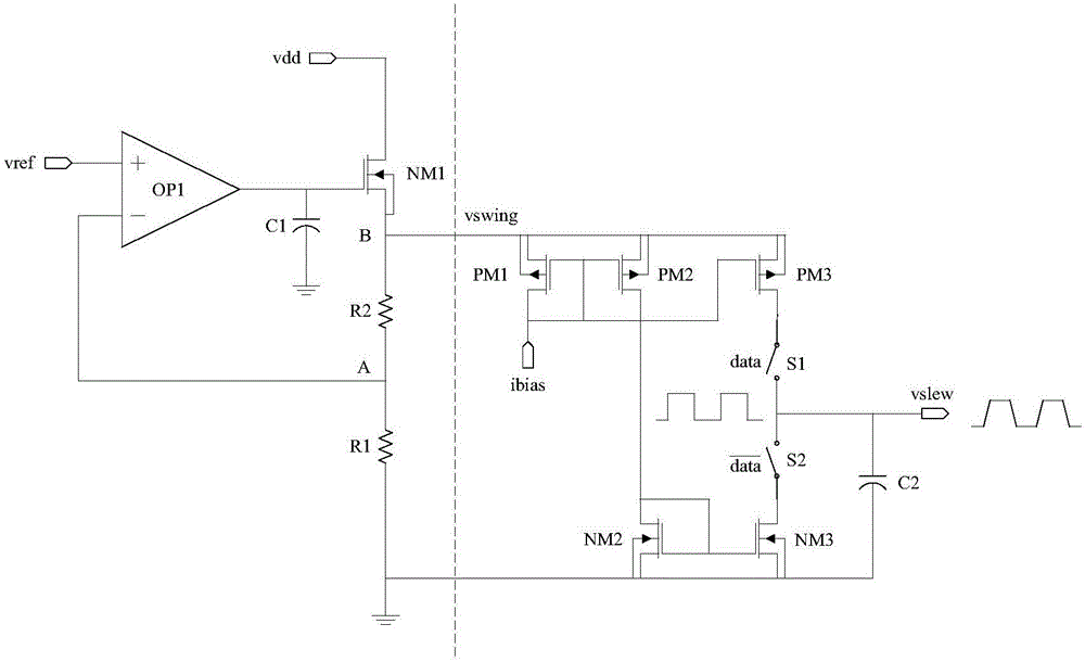
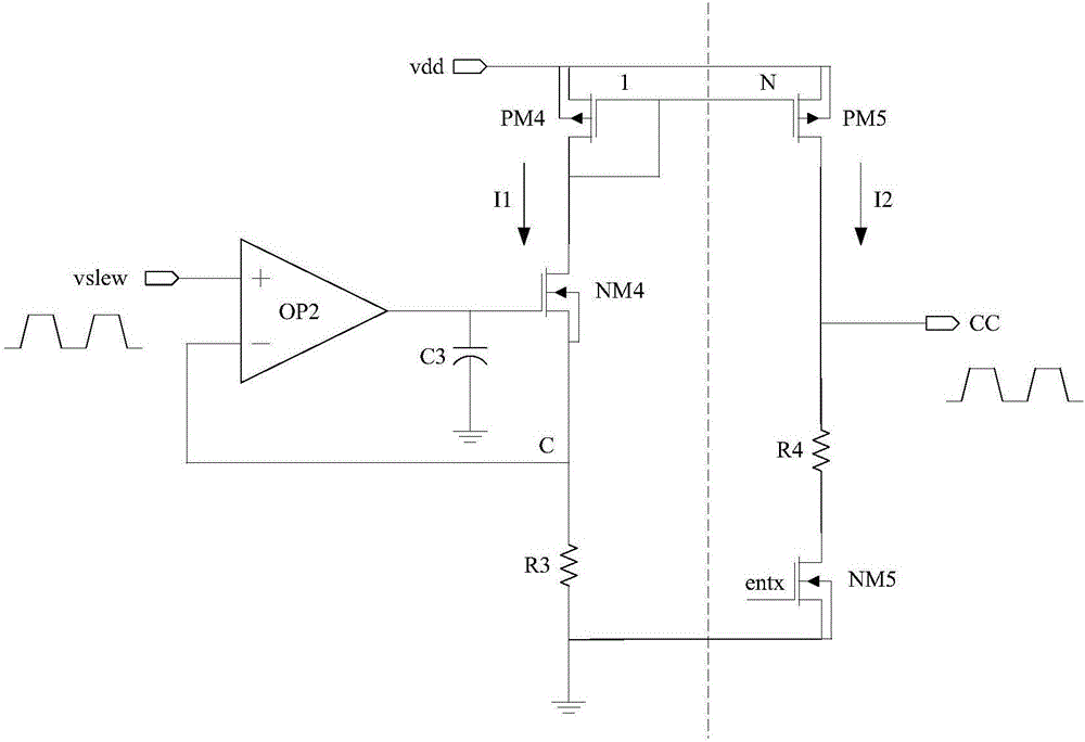
[0032] Specific embodiment one: such as figure 2 As shown, the circuit of the signal amplitude setting module and the conversion rate control module includes a first amplifier OP1, a first NMOS tube NM1, a first resistor R1, a second resistor R2, a first capacitor C1, and a first PMOS tube forming a negative feedback loop. PM1, the second PMOS tube PM2, the third PMOS tube PM3, the second NMOS tube NM2, the third NMOS tube NM3, the first switch S1, the second switch S2 and the second capacitor C2. The non-inverting terminal of OP1 is connected to the external reference voltage vref , The output terminal is connected to the gate of NM1, the drain of NM1 is connected to the power supply, the source is connected in series with R2 and R1, the other end of R1 is grounded, the negative phase end of OP1 is connected to the line between R1 and R2, the first end of C1 Connect the OP1 output terminal, the second terminal of C1 is grounded, the source of PM1, the source of PM2 and the sou...
specific Embodiment 2
[0036] Specific embodiment two: such as Figure 4 As shown, the circuit of the signal amplitude setting module and the conversion rate control module includes a third amplifier OP3, a sixth PMOS tube PM6, a seventh PMOS tube PM7, an eighth PMOS tube PM8, a ninth PMOS tube PM9, and a sixth NMOS tube NM6, The seventh NMOS tube NM7, the fourth capacitor C4, the fifth capacitor C5, the fifth resistor R5, the sixth resistor R6, the third switch S3, and the fourth switch S4. The non-phase terminal of OP3 is connected to the external reference voltage vdd- relative to the power supply. vref, the output terminal is connected to the PM6 grid, the PM6 source is connected in series with R6 and R5, the other end of R5 is connected to the power source, the PM6 drain is grounded, the negative phase terminal of OP3 is connected to the connection line of R5 and R6, and the output terminal of OP3 is also connected to C4 The first end, the other end of C4 is connected to the power supply, PM7 sou...
PUM
 Abstract
Description
Claims
Application Information


