A mbist clock optimization method and device

An optimization device and optimization method technology, which is applied in the detection of faulty computer hardware, function inspection, etc., can solve the problems of insufficient test power supply, high power consumption, and unstable test.

Active Publication Date: 2016-11-02
FUZHOU ROCKCHIP SEMICON
View PDF4 Cites 0 Cited by
  • Summary
  • Abstract
  • Description
  • Claims
  • Application Information

AI Technical Summary

Problems solved by technology

[0005] For this reason, it is necessary to provide a technical solution for mbist clock optimization to solve the problems of large power consumption, insufficient test power supply, and unstable test when performing mbist test due to the multiplexing of the working clock of the functional logic circuit in the existing chip. And other issues

Method used


Image

  • A mbist clock optimization method and device
  • A mbist clock optimization method and device

Examples


Embodiment Construction

[0033] In order to explain in detail the technical content, structural features, achieved goals and effects of the technical solution, the following will be described in detail in conjunction with specific embodiments and accompanying drawings.

[0034] DVFS (Dynamic Voltage and Frequency Scaling) dynamic voltage and frequency adjustment is a real-time voltage and frequency adjustment technology. Power consumption in CMOS circuits can be mainly divided into dynamic power consumption and static power consumption, the formula is as follows:

[0035] Power=∑(CV 2 αf+VI dq )

[0036] Among them, C represents the capacitance of the load capacitor, V is the operating voltage, α is the flip rate at the current clock frequency, f is the operating frequency, and I_dq represents the quiescent current. The first part of the formula represents the dynamic power consumption, and the latter part represents the static power consumption. It can be seen from the formula that if you want to...


PUM


Abstract

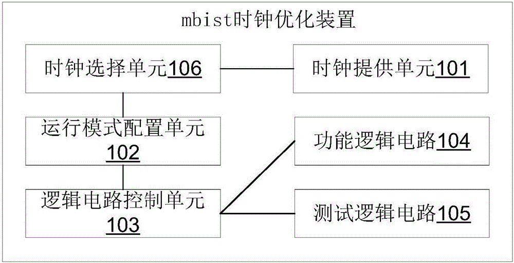
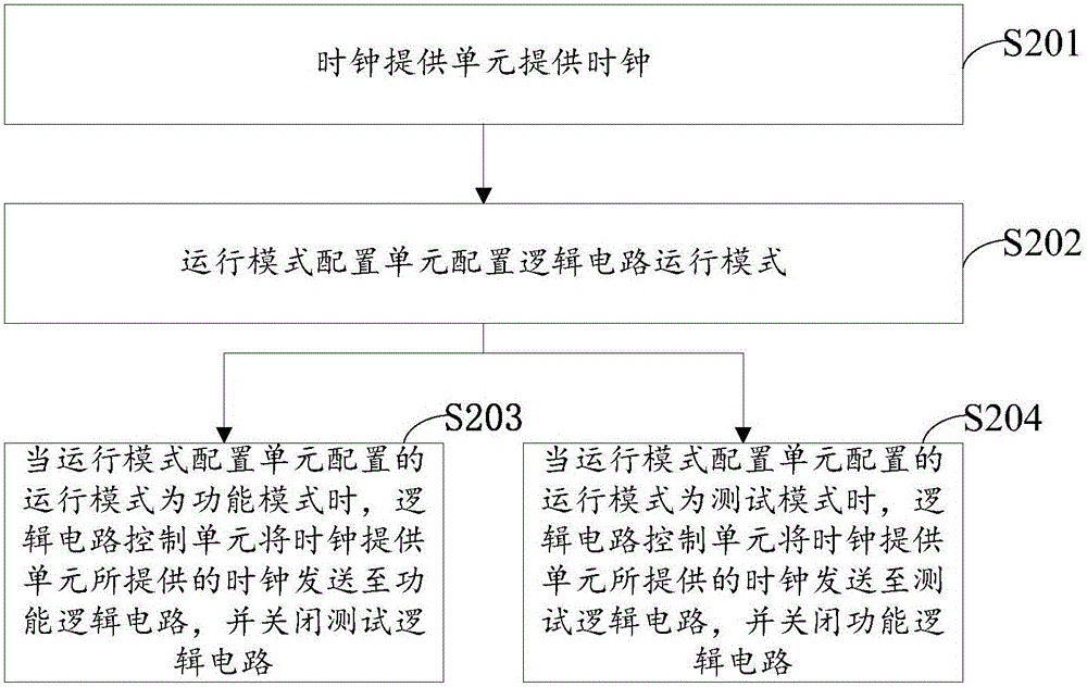
The present invention discloses a mbist clock optimization method and device wherein the method comprises the following steps: firstly, a clock providing unit provides a clock; and after that, a running mode configuration unit configures a logic circuit running mode, wherein the running mode comprises a function mode and a test mode; when the running mode configured by the running mode configuration unit is in the function mode, the logic circuit control unit sends the clock provided by the clock providing unit to a functional logic circuit and turns off the test logic circuit; when the running mode configured by the running mode configuration unit is in the test mode, the logic circuit control unit sends the clock provided by the clock providing unit to the test logic circuit and turns off the functional logic circuit. As the functional logic circuit and test logic circuit are completely separate, when a logic circuit is in working condition, the other logic circuits can be completely closed, thereby greatly reducing the consumption of chips in mbist tests and enhancing the stability of the tests.

Description

technical field [0001] The invention relates to the field of SOC chip design, in particular to an mbist clock optimization method and device. Background technique [0002] MBIST is the memory (memory) built-in self-test, which is the main test method for the internal memory of the chip. It embeds the test vector generation circuit and the comparison circuit into the chip, and only through a few simple peripheral control signals to start the internal memory. The test circuit automatically realizes the memory test, and automatically outputs the test comparison result after the test is completed. [0003] At present, the working clock of the memory test circuit is directly sharing the clock of the functional logic module. The advantage of this is that the clock of the functional circuit can be directly multiplexed without adding an additional clock structure, but this also leads to the memory test. The clocks of other non-mbist test circuits (that is, functional module logic b...

Claims


Application Information

Patent Timeline
Patent Type & Authority Applications(China)
IPC IPC(8): G06F11/27
CPCG06F11/27
Inventor 严云锋
Owner FUZHOU ROCKCHIP SEMICON
Why Eureka
Try Eureka