Wide visual angle mode TFT substrate manufacturing method

A substrate preparation and wide viewing angle technology, which is applied in semiconductor/solid-state device manufacturing, electrical components, electrical solid-state devices, etc., can solve problems such as reducing the yield of finished products and affecting electrical and optical properties

Inactive Publication Date: 2016-11-09
TRULY HUIZHOU SMART DISPLAY
View PDF4 Cites 0 Cited by
  • Summary
  • Abstract
  • Description
  • Claims
  • Application Information

AI Technical Summary

Problems solved by technology

[0004] The inventor found in research that the conventional technology has at least the following problems: in the process of using PECVD to make the PA layer, the process gas forming the PA layer will form a plasma, which contains a large amount of H ions and electrons, H ions and these Electrons may undergo a reduction reaction with the exposed first ITO layer of the substrate, thereby affecting the electrical and optical properties of the first ITO layer of the final wide viewing angle TFT substrate, reducing the yield of the finished product

Method used


Image

  • Wide visual angle mode TFT substrate manufacturing method
  • Wide visual angle mode TFT substrate manufacturing method
  • Wide visual angle mode TFT substrate manufacturing method

Examples


Embodiment Construction

[0033] In order to make the object, technical solution and advantages of the present invention clearer, the present invention will be further described in detail below in conjunction with the accompanying drawings and embodiments. It should be understood that the specific embodiments described here are only used to explain the present invention, not to limit the present invention.

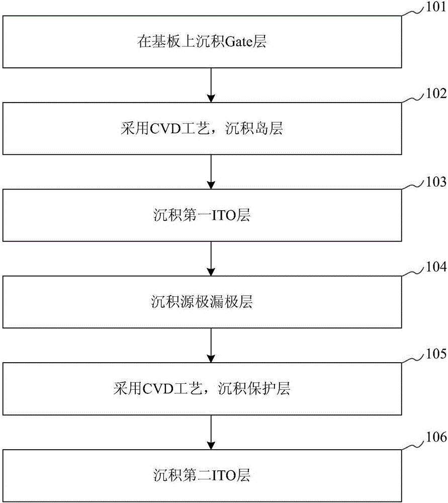
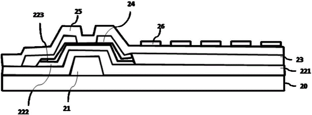
[0034] see figure 1 and figure 2 In one embodiment, a method for preparing a TFT substrate with a wide viewing angle mode is provided, including:

[0035] 101. A process of depositing a Gate layer on a substrate.

[0036] Specifically, a PVD (Physical Vapor Deposition, physical vapor deposition) film forming process can be used to deposit metal on the substrate 20 , and the Gate pattern 21 can be obtained through process treatment.

[0037] 102. A process of depositing an island layer by using a CVD process.

[0038] Specifically, the island (Island) layer is a non-metal film layer, including ...


PUM


Abstract

The invention discloses a wide visual angle mode TFT substrate manufacturing method. The method includes the steps of depositing a Gate layer on a substrate, depositing an island layer by employing CVD technology, depositing a first ITO layer, depositing a source-drain electrode layer, depositing a PA layer by employing PECVD technology, and depositing a second ITO layer, wherein the step of depositing a PA layer by employing PECVD technology includes dissociating the process gas in the step with relative low power into plasma, reacting to deposit a first PA layer, and dissociating the process gas in the step with relative high power into plasma and reacting to deposit a second PA layer. In the manufacturing process, reduction of the first ITO layer can be prevented, and the electric and optical performance of the first ITO layer can be protected. The transmittance of the TFT substrate can be improved, and the power consumption of a TFT display is reduced.

Description

technical field [0001] The invention relates to the fields of semiconductor device preparation and display, in particular to a method for preparing a TFT substrate with a wide viewing angle mode. Background technique [0002] TFT LCD (Thin-Film-Transistor Liquid Crystal Display, Thin-Film-Transistor Liquid Crystal Display) has been widely used due to its high speed, high brightness, high contrast and other advantages. There are many modes of TFT substrates, the more common ones are TN, IPS, MVA and so on. TN mode has the fastest response speed, but the worst color, relatively small viewing angle, and low cost. It is mainly used in monitors and small TVs. The TFT substrate of wide viewing angle mode can reach a viewing angle of more than 170°. The typical IPS mode has a relatively high viewing angle, fast response speed, accurate color, and moderate cost. [0003] In the traditional technology, the TFT substrate of the wide viewing angle mode needs to go through multiple pr...

Claims


Application Information

Patent Timeline
Patent Type & Authority Applications(China)
IPC IPC(8): H01L21/77H01L27/12
CPCH01L27/1259
Inventor 朱东梅刘力明邓泽新黄伟东李建华
Owner TRULY HUIZHOU SMART DISPLAY
Why Eureka
Try Eureka