Microstrip array antenna loaded with graphene decoupling network

A decoupling network and microstrip array technology, applied in the directions of antenna, antenna coupling, antenna array, etc., can solve the problems of large size of microstrip array antenna and poor unit isolation, and achieve the effect of improving isolation.

Active Publication Date: 2016-11-09
GUILIN UNIV OF ELECTRONIC TECH
View PDF4 Cites 5 Cited by
  • Summary
  • Abstract
  • Description
  • Claims
  • Application Information

AI Technical Summary

Problems solved by technology

[0004] The technical problem to be solved by the present invention is that the existing microstrip array antenna has the problems of large size and poor unit isolation. It provides a microstrip array antenna loaded with a graphene decoupling network, which can effectively reduce the radiation patch in the microstrip array antenna. Electromagnetic coupling between, thus realizing the compact structure of the array antenna

Method used


Image

  • Microstrip array antenna loaded with graphene decoupling network
  • Microstrip array antenna loaded with graphene decoupling network
  • Microstrip array antenna loaded with graphene decoupling network

Examples


Embodiment Construction

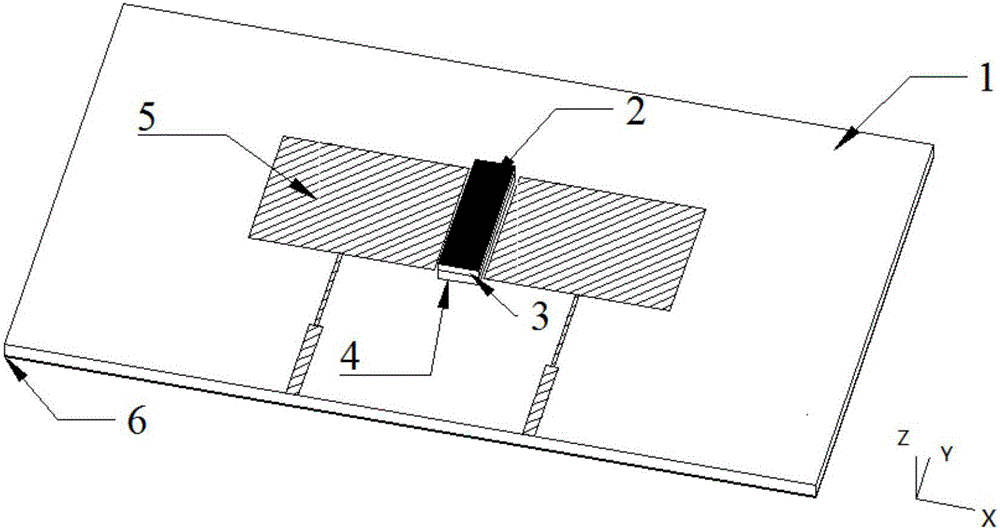
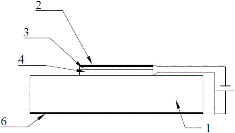
[0023] A microstrip array antenna loaded with a graphene-2 ​​decoupling network, such as figure 1 with 2 As shown, it consists of a dielectric board 1 , a metal floor 6 , and more than two independent antenna array units 5 . The metal floor 6 and the antenna array unit 5 can be located on the same side surface of the dielectric board 1 , or can be located on different side surfaces of the dielectric board 1 . In a preferred embodiment of the present invention, the metal floor 6 is located on the lower surface of the dielectric board 1 , and all the antenna array units 5 are located on the upper surface of the dielectric board 1 .

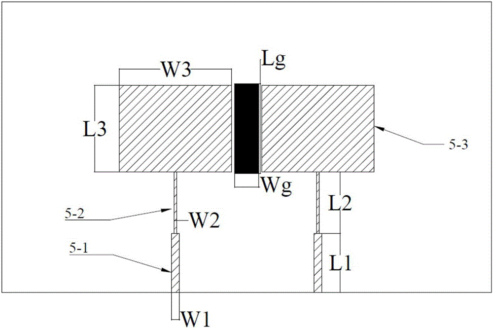
[0024] The dielectric board 1 is used as the dielectric board 1 of the array antenna, with a length×width×thickness of 160mm×95mm×0.8mm, a relative permittivity of 4.4, and a loss tangent of 0.02. The distance between the edge of the dielectric plate 1 and the edge of the radiation patch 5-3 is slightly greater than a quarter of a wavelength, so t...


PUM


Abstract

The invention discloses a microstrip array antenna loaded with a graphene decoupling network. The microstrip array antenna comprises a medium plate and a metallic floor and more than two mutually independent antenna array units covered on the surface of the medium plate, wherein a graphene layer is arranged between two adjacent antenna array units and covered on the medium plate, a gap is formed between the graphene layer and the antenna array units, and the graphene layer is connected with an external DC offset voltage. Electromagnetic coupling between radiation pasters in the microstrip array antenna can be effectively reduced to realize compact structure of an array antenna.

Description

technical field [0001] The invention relates to the technical field of antennas and metamaterials, in particular to a microstrip array antenna loaded with a graphene decoupling network. Background technique [0002] Microstrip array antennas have been widely used in wireless communication systems such as aircraft, satellites, and missiles because of their light weight, low cost, easy processing, and convenience for conformal shapes. However, it is generally believed that the spacing between the elements of the microstrip array antenna should be greater than one-half of the wavelength in order to avoid the coupling interaction between the radiating elements and ensure the radiation performance of the antenna. However, size-constrained communication devices often cannot provide the spacing required by microstrip array antennas. Therefore, judging from the current demand for antennas, size has already become a decisive factor for antenna applications. [0003] At present, the ...

Claims


Application Information

Patent Timeline
Patent Type & Authority Applications(China)
IPC IPC(8): H01Q1/52H01Q21/00
CPCH01Q1/52H01Q1/523H01Q21/00
Inventor 高喜乔玮杨万里李思敏曹卫平姜彦南于新华
Owner GUILIN UNIV OF ELECTRONIC TECH
Why Eureka
Try Eureka