Monocrystalline silicon wafer texture surface making additive and application

A monocrystalline silicon wafer and additive technology, applied in the direction of single crystal growth, single crystal growth, crystal growth, etc., can solve the problems of slow reaction speed, increase battery efficiency, and decrease production capacity, so as to reduce reflectivity, improve battery efficiency, The effect of increased productivity

Active Publication Date: 2016-11-16
CHANGZHOU SHICHUANG ENERGY CO LTD
View PDF5 Cites 24 Cited by
  • Summary
  • Abstract
  • Description
  • Claims
  • Application Information

AI Technical Summary

Problems solved by technology

This texturing process is more suitable for mortar sheets, but with the popularity of diamond wire cut silicon wafers, the above texturing process can no longer meet the needs of production lines
[0003] Compared with traditional mortar sheets, silicon wafers cut by diamond wire have heavy traces, small damage layer, and slow reaction speed. If conventional texturing additives are still used, the texturing time will be too long, the production capacity will be reduced, and the uniformity of the texturing pyramid will be uneven. Well, not conducive to further improving battery efficiency

Method used


Image

  • Monocrystalline silicon wafer texture surface making additive and application

Examples


Embodiment Construction

[0026] The specific implementation manners of the present invention will be further described below in conjunction with the drawings and examples. The following examples are only used to illustrate the technical solution of the present invention more clearly, but not to limit the protection scope of the present invention.

[0027] The technical scheme of concrete implementation of the present invention is:

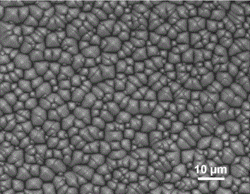
[0028] A method for making texture of a monocrystalline silicon wafer, the specific steps comprising:

[0029] 1) Prepare texturing additives: add 0.1% to 30% by mass of component A and 0.01% to 10% of component B into the remaining water, mix evenly to make texturing additives;

[0030] 2) Prepare the texturing liquid: add the texturing additive prepared in step 1) to the alkaline solution, mix evenly to prepare the texturing liquid; the mass ratio of the texturing additive to the alkaline solution is 0.2-5:100; Described alkali solution is the aqueous solution of inorg...


PUM


Abstract

The invention provides a monocrystalline silicon wafer texture surface making additive. The monocrystalline silicon wafer texture surface making additive comprises the following components in percentages by mass: 0.1%-3% of a component A, 0.01%-10% of a component B and the balance of water. The component A is selected from one or more of crown ether, crown ether derivatives and alkali metal complex of the crown ether; and the component B is alcohol ether. The invention further provides texture surface making liquid for monocrystalline silicon wafer texture surface making. The texture surface making liquid contains an alkali solution and the monocrystalline silicon wafer texture surface making additive. The invention further provides a monocrystalline silicon wafer texture surface making method. Texture surface making on a monocrystalline silicon wafer is carried out by the texture surface making liquid. The additive is added in the monocrystalline silicon wafer texture surface making liquid, so that texture surface making reaction becomes fast, quick texture surface making on the monocrystalline silicon wafer cut by a diamond wire can be carried out, the capacity is improved, uniform and compact texture surface pyramids can be obtained, the reflectivity is reduced, and the efficiency of a battery is improved.

Description

technical field [0001] The invention relates to a monocrystalline silicon wafer texturing additive and its application. Background technique [0002] At present, the conventional texturing process of monocrystalline silicon wafers generally uses sodium hydroxide or potassium hydroxide, and appropriately adds non-alcoholic texturing additives for texturing. This texturing process is more suitable for mortar sheets, but with the popularity of diamond wire cut silicon wafers, the above texturing process can no longer meet the needs of production lines. [0003] Compared with traditional mortar sheets, silicon wafers cut by diamond wire have heavy traces, small damage layer, and slow reaction speed. If conventional texturing additives are still used, the texturing time will be too long, the production capacity will be reduced, and the uniformity of the texturing pyramid will be uneven. Well, not conducive to further improving battery efficiency. Contents of the invention [...

Claims


Application Information

Patent Timeline
Patent Type & Authority Applications(China)
IPC IPC(8): C30B33/10C30B29/06
CPCC30B29/06C30B33/10
Inventor 陈培良符黎明
Owner CHANGZHOU SHICHUANG ENERGY CO LTD
Why Eureka
Try Eureka