
Optical alignment method for processing plate products
A product and optical technology, which is applied in the field of optical alignment of board products, can solve the problems of expensive equipment, high maintenance costs, and high equipment installation requirements, and achieve short alignment time, high production accuracy, and high alignment accuracy. Effect
- Summary
- Abstract
- Description
- Claims
- Application Information
AI Technical Summary
Problems solved by technology
Method used
Image

Examples
Embodiment 1
[0049] Embodiment 1 of the present invention provides an optical alignment method for processing board products, including:
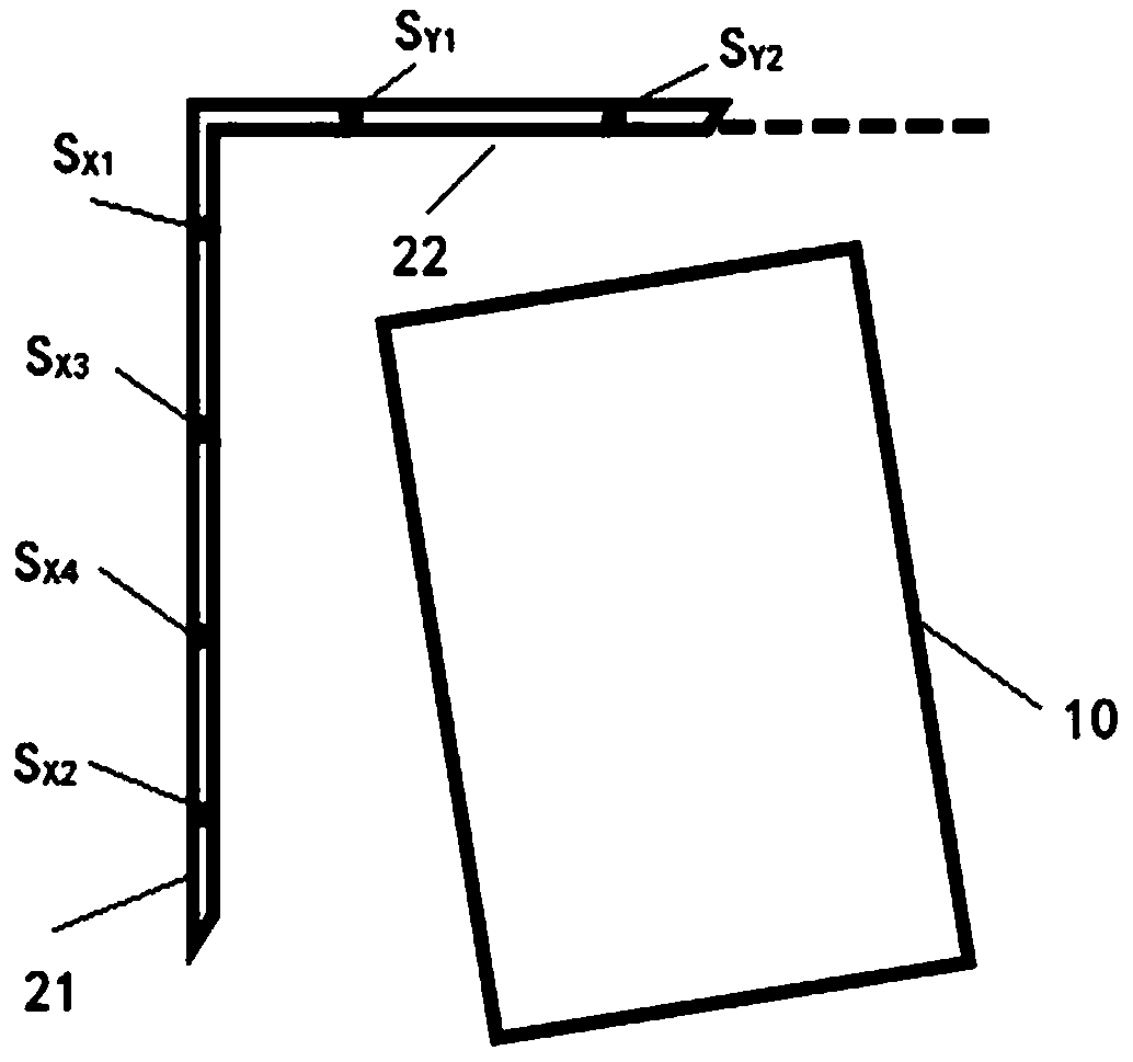
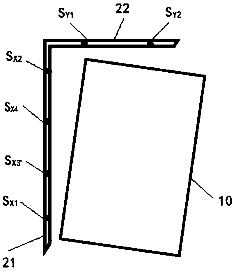
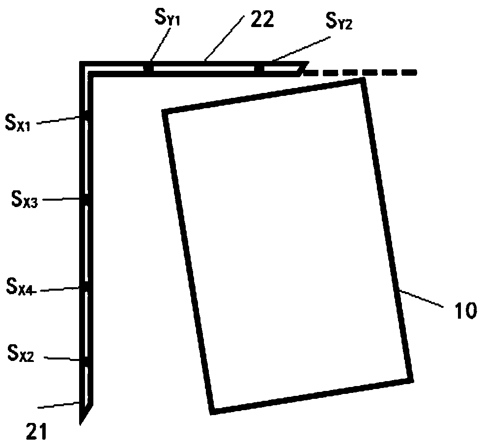
[0050] Step 1: Set up an L-shaped photoelectric test platform. The L-shaped photoelectric test platform is provided with an X-axis and a Y-axis, and at least two photoelectric sensors are arranged on the X-axis and the Y-axis;
[0051] Step 2: Fix the substrate 10 to be processed (which can be rectangular or square) on the stage, and the original state of the substrate 10 to be processed is fixed on the stage as figure 1 and figure 2 shown. Below to figure 1 For example, the stage drives the substrate 10 to be processed to rotate and move through the rotary movement mechanism provided below, and the state is as follows image 3 As shown, the stage drives the substrate 10 to be processed to move along the X-axis direction of the L-shaped photoelectric test platform to any photoelectric sensor S on the Y-axis 22 of the L-shaped photoelectric test plat...
Embodiment 2
[0073] Embodiment 2 of the present invention also provides an optical alignment method for processing plate products, including:
[0074] Step 1: Set up a photoelectric test matrix platform, the photoelectric test matrix platform is provided with M rows and N columns of photoelectric sensor monitoring points along the X and Y directions, wherein M>1, N>1, and each row and column is equipped with at least 2 photoelectric sensors such as Figure 9 shown;
[0075] Step 2: Fix the substrate 10 to be processed on the stage, and the stage drives the substrate 10 to be processed to rotate and move through the rotary movement mechanism provided below, and drives the substrate 10 to be processed along the X axis of the photoelectric test matrix platform. Move in the direction until the state of any photoelectric sensor in the first row of the photoelectric test matrix platform changes from OFF to ON;
[0076] Step 3: Drive the stage to move the substrate 10 to be processed along the ...
PUM
 Abstract
Description
Claims
Application Information