
A Method for Optimizing the Insulating Layer of Organic Thin Film Transistors by Double Crosslinking Reaction

An organic thin film and insulating layer technology, applied in the field of optimizing the insulating layer of organic thin film transistors, can solve problems such as affecting device performance, easy aging, and non-densification, and achieve the effects of simple operation, low cost, and good optoelectronic performance.

Active Publication Date: 2018-08-17
FUZHOU UNIV
View PDF4 Cites 0 Cited by
  • Summary
  • Abstract
  • Description
  • Claims
  • Application Information

AI Technical Summary

Problems solved by technology

Although organic insulating materials have many advantages, there are disadvantages such as easy aging and non-denseness of organic insulating materials, which affect the performance of devices.

Method used


Image

  • A Method for Optimizing the Insulating Layer of Organic Thin Film Transistors by Double Crosslinking Reaction
  • A Method for Optimizing the Insulating Layer of Organic Thin Film Transistors by Double Crosslinking Reaction
  • A Method for Optimizing the Insulating Layer of Organic Thin Film Transistors by Double Crosslinking Reaction

Examples


Embodiment 1

[0081] 1) Clean a P-type silicon wafer with a size of 1.5cm×2cm with acetone, isopropanol, chloroform, and distilled water (three times), and then dry it with nitrogen to obtain a clean silicon wafer as a gate.

[0082] 2) Use a syringe with a 0.22um filter plug to spread the 150mg / ml PVP solution over the silicon wafer, and then use a speed of 2000rpm (30s) to make the PVP solution form a uniform film on the silicon wafer, and then move the silicon wafer into the glove box for further processing. A 850nm insulating layer film was prepared by cross-linking reaction at 120°C (2h).

[0083] 3) The semiconductor polymer PDVT-8 was dissolved in chloroform at 5 mg / ml, and the PDVT-8 solution was spin-coated at 1000 rpm (60 s) to prepare the active layer, and then heated at 150 °C for 10 min.

[0084] 4) Finally, a 50nm-thick source-drain electrode with a channel length of 30um and a width of 1mm was evaporated on the silicon wafer obtained in step 5) by thermal evaporation using a ...

Embodiment 2

[0086] 1) Clean a P-type silicon wafer with a size of 1.5cm×2cm with acetone, isopropanol, chloroform, and distilled water (three times), and then dry it with nitrogen to obtain a clean silicon wafer as a gate.

[0087] 2) Use a syringe with a 0.22um filter plug to spread the 150mg / ml PVP solution over the silicon wafer, and then use a speed of 2000rpm (30s) to make the PVP solution form a uniform film on the silicon wafer, and then move the silicon wafer into the glove box for further processing. A 850nm insulating layer film was prepared by cross-linking reaction at 120°C (2h).

[0088] 3) Drop the methacrylic acid (MAA) small molecule monomer solution on the sample that has prepared the insulating layer film, among which, MAA liquid small molecule monomer: EGDMA: photoinitiator Irgacure 651=96:3:1, static After 2s, use 5000rpm (60) to remove excess small molecule monomer solution on the surface of the insulating layer.

[0089] 4) Prepare a 40w-BL Philips UV lamp, and place ...

Embodiment 3

[0094] 1) A P-type silicon wafer with a size of 1.5cm×2cm was blown dry with acetone, isopropanol, chloroform, distilled water (three times) and nitrogen to obtain a clean silicon wafer as a gate.

[0095] 2) Use a syringe with a 0.22um filter plug to spread the 150mg / ml PVP solution over the silicon wafer, and then use a speed of 2000rpm (30s) to make the PVP solution form a uniform film on the silicon wafer, and then move the silicon wafer into the glove box for further processing. A 850nm insulating layer film was prepared by cross-linking reaction at 120°C (2h).

[0096] 3) Drip the small molecule monomer solution of methyl methacrylate (MMA) on the sample that has prepared the insulating layer film, among which, MMA liquid small molecule monomer: EGDMA: photoinitiator Irgacure 651=96:3:1 After standing for 2s, use 5000rpm (60s) to remove excess small molecule monomer solution on the surface of the insulating layer.

[0097] 4) Prepare a 40w-BL Philips UV lamp, and place ...


PUM


Abstract

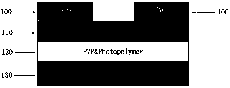
The invention relates to a method for optimizing the insulating layer of an organic thin film transistor through double crosslinking reactions, and provides an organic thin film transistor, which includes a substrate, an insulating layer, an active layer, and source and drain electrodes arranged in sequence from bottom to top ; After the insulating layer is formed on the grid in the substrate by using a solution method and using a spin coating process or a scraping process, the liquid organic small molecule monomer solution is infiltrated into the insulating layer, and treated with UV light. The small molecular monomers in the small molecular monomer solution are polymerized and solidified to be embedded in the network structure of the insulating layer to modify the surface of the insulating layer. The method for modifying the surface of the insulating layer proposed by the invention has simple and convenient operation methods and obvious modification effect, can effectively reduce the leakage current of the organic thin film transistor and improve the mobility of the organic thin film transistor.

Description

technical field [0001] The invention relates to the field of electro-optical materials, in particular to a method for optimizing the insulating layer of an organic thin film transistor by injecting an interpenetrating network polymer into the surface. Background technique [0002] As an important part of the organic thin film transistor, the insulating layer mainly plays the role of isolating the gate and the active layer or the source and drain electrodes. The layer forms a good contact surface and cannot affect the growth of the active layer film. Both inorganic materials and organic materials can be used to prepare insulating layers in organic thin film transistors. The most commonly used of these is SiO 2 , it has good insulating properties, but it cannot form a good contact interface with the organic film, and it needs to be modified when preparing the active layer on it. In addition, the preparation of SiO 2 Generally, the thermal growth method is adopted, and the p...

Claims


Application Information

Patent Timeline
Patent Type & Authority Patents(China)
IPC IPC(8): H01L51/05H01L51/40
CPCH10K10/478H10K10/471
Inventor 陈惠鹏郭太良张军张国成陈赐海杨辉煌
Owner FUZHOU UNIV
Learn More