Manufacturing method of polytetrafluoroethylene dielectric circuit board with multilayered dielectric circuits
A polytetrafluoroethylene, circuit board manufacturing technology, applied in the direction of multilayer circuit manufacturing, printed circuit manufacturing, printed circuit, etc., to achieve the effect of improving surface roughness and realizing the problem of interlayer bonding
- Summary
- Abstract
- Description
- Claims
- Application Information
AI Technical Summary
Problems solved by technology
Method used
Image

Examples
Embodiment 1
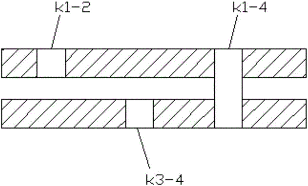
[0019] Example 1 as figure 1 Shown, a polytetrafluoroethylene dielectric circuit board manufacturing method of a multilayer dielectric circuit comprises the steps:
[0020] Step (1), select two PTFE resin double panels;
[0021] Step (2), bake the first PTFE resin double-sided board, CNC drilling, plasma technology treatment, hole metallization, and realize the first side and the second PTFE double-sided board of the first PTFE resin Two-sided interconnection, as attached figure 1 In the K1-2 interconnection, the inner layer circuit pattern is made on the second side of the first polytetrafluoroethylene resin double-sided board; the process of making the inner layer circuit pattern is: pattern transfer, copper plating on the hole, pattern transfer , Hole electroplating and etching graphics;
[0022] Step (3), bake the second PTFE resin double-sided panel, CNC drilling, plasma treatment, and metallization of the hole to realize the first and second sides of the second PTFE r...
PUM
 Abstract
Description
Claims
Application Information
 - R&D
- Intellectual Property
- Life Sciences
- Materials
- Tech Scout
- Unparalleled Data Quality
- Higher Quality Content
- 60% Fewer Hallucinations
Browse by: Latest US Patents, China's latest patents, Technical Efficacy Thesaurus, Application Domain, Technology Topic, Popular Technical Reports.
© 2025 PatSnap. All rights reserved.Legal|Privacy policy|Modern Slavery Act Transparency Statement|Sitemap|About US| Contact US: help@patsnap.com