Photosynthetic apparatus
A photosynthesis and semiconductor technology, applied in reduction and oxidation devices, photovoltaic power generation, electrolytic organic production, etc., can solve problems such as attenuation and widening of the interval between water tanks 920
- Summary
- Abstract
- Description
- Claims
- Application Information
AI Technical Summary
Problems solved by technology
Method used
Image

Examples
no. 1 Embodiment approach 〕
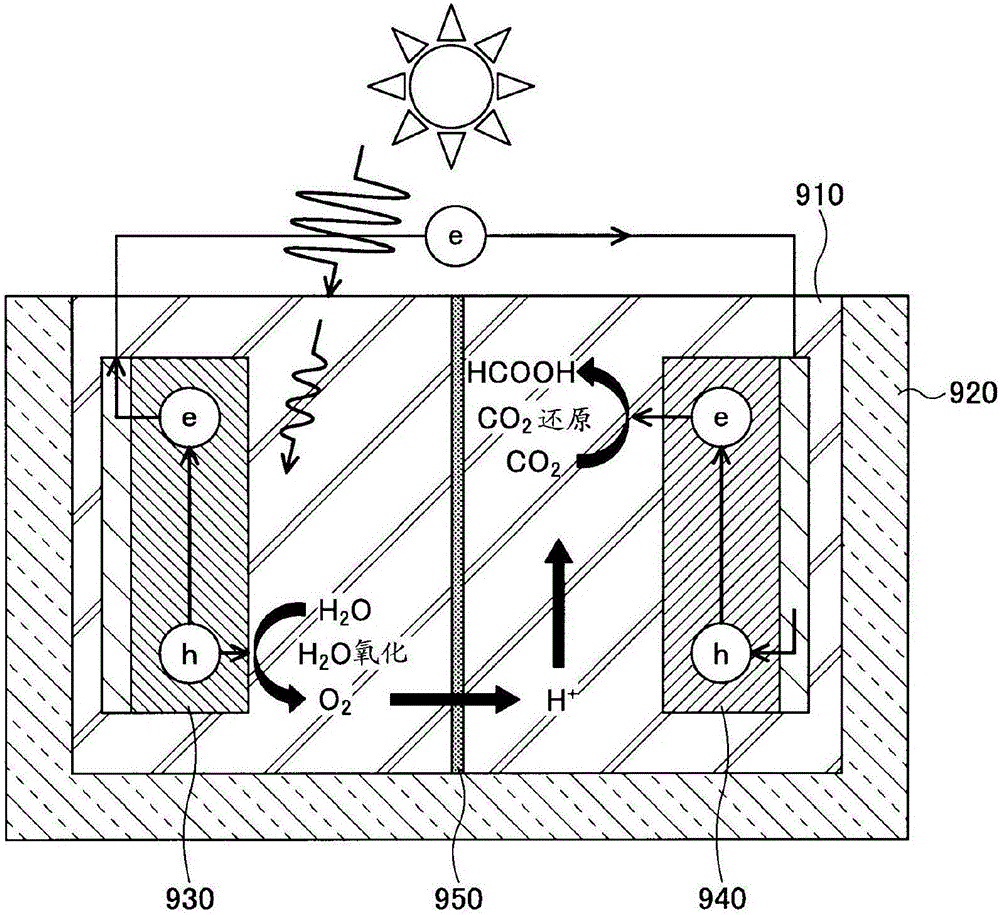
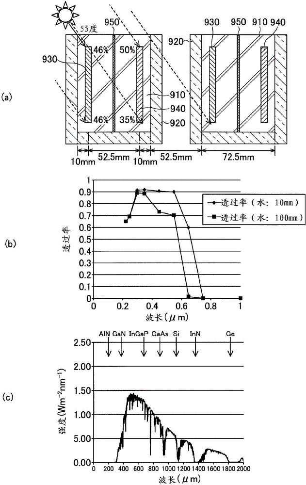
[0060] Incidentally, as figure 2 As shown in (c), in the solar spectrum, the intensity of light having a wavelength of 0.3 μm to 1.1 μm is high. Since this wavelength range corresponds to the band gap of semiconductor materials such as Si, GaAs, and GaN, it is possible to manufacture a light synthesis device using these semiconductor materials.
[0061] (photosynthesis device)
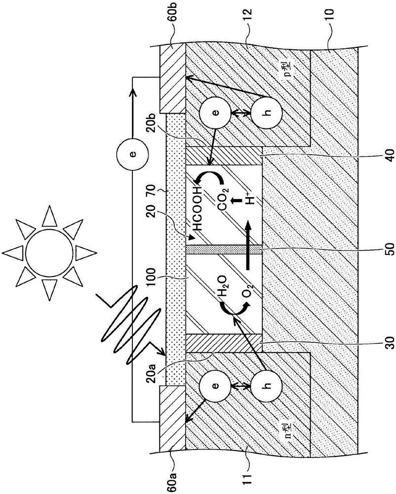
[0062] Next, for the photosynthesis device in this embodiment, based on image 3 Be explained. image 3 It is a cross-sectional view of the photosynthesis device in this embodiment. In the light synthesis device in the present embodiment, grooves 20 are formed on the surface of a semiconductor substrate 10 made of Si (silicon). The water 100 containing carbon dioxide is supplied to the tank part 20, and the tank part 20 is a microchannel water tank which becomes a flow path through which the water 100 containing carbon dioxide flows. In this embodiment, the groove portion 20 is formed of a groove...
no. 2 Embodiment approach 〕
[0092]Next, a second embodiment will be described. Incidentally, in the photosynthesis device in the first embodiment, Si is used as a semiconductor material, but similar to solar cells and the like, since Si is an indirect transition type semiconductor, solar light energy conversion efficiency decreases. On the other hand, direct transition semiconductors such as GaAs, InP, and GaN are superior in solar light energy conversion efficiency to Si. In the case of using Si as the semiconductor material, ion implantation is used to form the pn junction, but in the case of using GaAs, InP, GaN, etc. as the semiconductor material, the pn junction is formed by regrowth.
[0093] (Manufacturing method of photosynthetic device)
[0094] Next, for the manufacturing method of the photosynthetic device in this embodiment, based on Figure 17 ~ Figure 24 Be explained. As an example, the photosynthesis device in this embodiment is a pn junction type photosynthesis device using GaN as a se...
no. 3 Embodiment approach 〕
[0112] Next, a third embodiment will be described. The photosynthesis device in this embodiment is a tandem junction type photosynthesis device in which an n-type region and a p-type region are formed by stacking a plurality of semiconductor layers with different band gaps.
[0113] based on Figure 25 The photosynthesis device in this embodiment will be described. also, Figure 25 (a) is a plan view of the transmissive surface coating film 170 in the photosynthesis device in this embodiment, Figure 25 (b) is in Figure 25 (a) The cross-sectional view cut|disconnected by the dashed-dotted line 25A-25B.
[0114] (photosynthesis device)
[0115] In this embodiment, a GaN layer 111 is formed on a semiconductor substrate 110, and an n-type region 210 and a p-type region formed by laminating materials with different bandgaps are formed on both sides of a groove portion 120 formed on the GaN layer 111. 220 photosynthesis device. Specifically, n-type region 210 is formed of s...
PUM
| Property | Measurement | Unit |
|---|---|---|
| thickness | aaaaa | aaaaa |
Abstract
Description
Claims
Application Information