Photoconductive diamond film switch

A photoconductive switch, diamond film technology, applied in semiconductor devices, electrical components, circuits, etc., can solve the problems of narrow wavelength range of excitation laser, limited application of photoconductive switch, insufficient voltage resistance, etc., to improve heat dissipation performance and fast response speed. , the effect of improving the pressure resistance

Active Publication Date: 2014-03-19
CHINA WEAPON EQUIP RES INST
View PDF0 Cites 7 Cited by
  • Summary
  • Abstract
  • Description
  • Claims
  • Application Information

AI Technical Summary

Problems solved by technology

[0005] But at the same time, most of the current photoconductive switches use coplanar electrode structures, and the withstand voltage performance is not high enough; the lifespan is generally not long enough, currently about a thousand times of pulse excitation; at the same time, beca

Method used


Image

  • Photoconductive diamond film switch
  • Photoconductive diamond film switch

Examples


Embodiment Construction

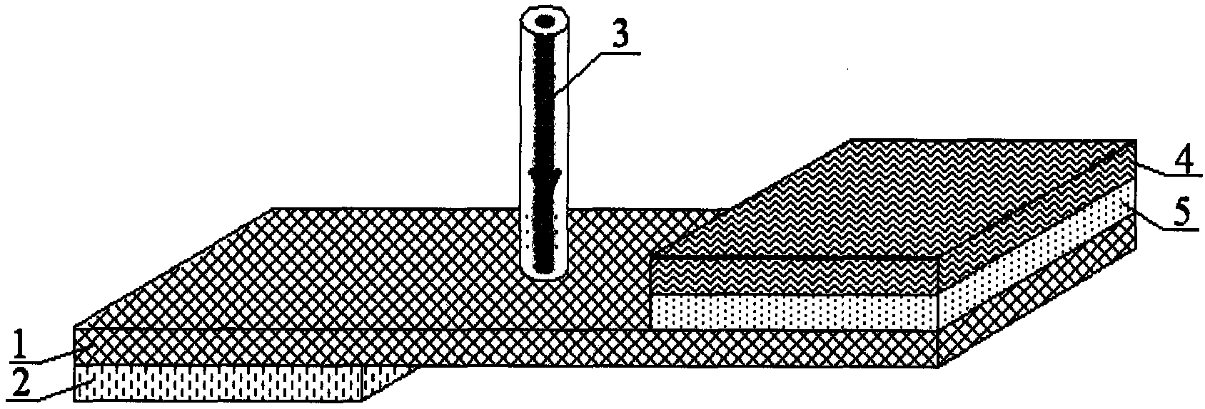
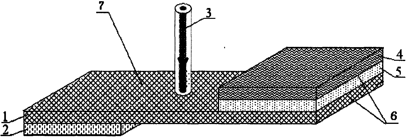
[0014] A photoconductive diamond film switch, comprising a semiconductor film 1, a photoconductive switch negative pole 4 and a photoconductive switch positive pole 2, the photoconductive switch negative pole 4 is connected to the semiconductor film 1, and the photoconductive switch positive pole 2 is connected to the semiconductor film 1, characterized in that, A layer of diamond film 5 is added between the negative electrode 4 of the photoconductive switch and the semiconductor film 1, the positive electrode 2 of the photoconductive switch and the negative electrode 4 of the photoconductive switch are respectively connected to both sides of the semiconductor film 1, and the positive electrode 2 of the photoconductive switch is separated from the negative electrode 4 of the photoconductive switch. distance.

[0015] A metal transition layer 6 is added between the negative electrode 4 of the photoconductive switch and the diamond film 5 and between the semiconductor thin film 1...


PUM


Abstract

The invention relates to a photoconductive diamond film switch, which belongs to the technical field of photoconductive switches, and specifically relates to a photoconductive switch device with a new structure. It includes a semiconductor film (1), a photoconductive switch negative pole (4) and a photoconductive switch positive pole (2), the photoconductive switch negative pole (4) is connected to the semiconductor film (1), and the photoconductive switch positive pole (2) is connected to the semiconductor film (1) ), which is characterized in that a layer of diamond film (5) is added between the photoconductive switch negative pole (4) and the semiconductor film (1), and the positive pole (2) of the photoconductive switch and the photoconductive switch negative pole (4) are respectively connected to the semiconductor film ( 1), and there is a distance between the positive pole (2) of the photoconductive switch and the negative pole (4) of the photoconductive switch. Compared with the traditional photoconductive switch, the service life is increased by an order of magnitude. Experiments show that the photoconductive switch of the present invention can be used nearly ten thousand times, which is greatly improved compared with the traditional photoconductive switch.

Description

technical field [0001] The invention belongs to the technical field of photoconductive switches, and in particular relates to a photoconductive switch device with a new structure. Background technique [0002] A photoconductive semiconductor switch (abbreviated as a photoconductive switch) is a three-terminal optoelectronic device that uses laser pulse energy to excite photoconductive (semiconductor) materials to cause a sudden change in conductivity, thereby generating electrical pulses. [0003] The photoconductive material of a photoconductive switch is usually a semiconductor. When there is no light, the switch is in the off state under the bias voltage. After the laser pulse is irradiated, photogenerated carriers are generated in the semiconductor material, forming a large number of electron-hole pairs, and the resistivity of the material drops suddenly, so that the switch is turned on instantaneously. The circuit outputs current pulses with high peak power. Since the ...

Claims


Application Information

Patent Timeline
IPC IPC(8): H01L31/16
Inventor 李伟冯晓波郭胜刚陈曦纪帆董海燕杨超王琦
Owner CHINA WEAPON EQUIP RES INST
Why Eureka
Try Eureka