How the transistor is formed

A transistor and process technology, applied in the field of semiconductor manufacturing, can solve the problems of poor electrical connection performance, reduced performance and reliability of semiconductor devices, etc., and achieve the effects of uniform distribution of sulfide ions and simple doping process

Active Publication Date: 2019-05-28
SEMICON MFG INT (SHANGHAI) CORP
View PDF3 Cites 0 Cited by
  • Summary
  • Abstract
  • Description
  • Claims
  • Application Information

AI Technical Summary

Problems solved by technology

[0004] However, the electrical connection between the stress layer and the conductive structure formed in the prior art is poor, which reduces the performance and reliability of semiconductor devices

Method used


Image

  • How the transistor is formed
  • How the transistor is formed
  • How the transistor is formed

Examples


Embodiment Construction

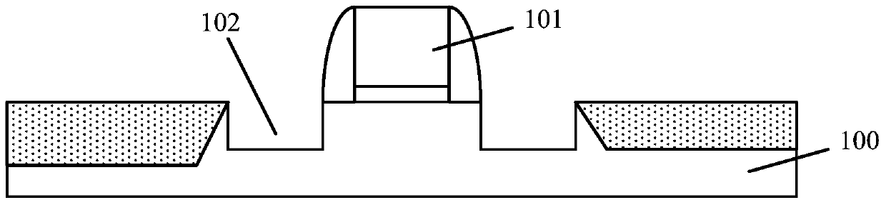
[0032] As mentioned in the background art, the electrical connection between the stress layer and the conductive structure formed in the prior art is poor, which reduces the performance and reliability of the semiconductor device.

[0033] After research, it is found that since the material of the stress layer is a semiconductor material, and the material of the conductive structure is metal, there is a Schottky barrier at the contact interface between the stress layer and the conductive structure, causing carriers to flow between the stress layer and the conductive structure. The transition at the contact interface of the structure is relatively difficult, and the contact resistance between the stress layer and the conductive structure is relatively large.

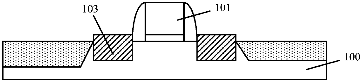
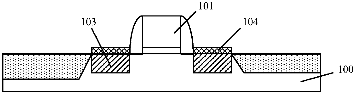
[0034] In order to reduce the contact resistance between the stress layer and the conductive structure, a method is to form an electrical contact layer made of metal silicide on the surface of the stress layer, and the met...


PUM

PropertyMeasurementUnit
thicknessaaaaaaaaaa
thicknessaaaaaaaaaa
thicknessaaaaaaaaaa

Abstract

The invention provides a transistor formation method, which comprises the following steps: providing a substrate; forming a gate structure on the surface of the substrate; forming an opening in the substrate at the two sides of the gate structure; forming a stress layer in the opening; forming a cover layer on the surface of the stress layer, wherein the cover layer is doped by oxygen family element ions; and through metal silicification process, converting the cover layer into an electric contact layer, wherein the electric contact layer is made of metal silicide doped by oxygen family element ions. According to the formed transistor, resistance of the surface of the stress layer is reduced, and working current of the transistor is improved, and performance thereof is stable.

Description

technical field [0001] The invention relates to the technical field of semiconductor manufacturing, in particular to a method for forming a transistor. Background technique [0002] With the rapid development of semiconductor manufacturing technology, semiconductor devices are developing towards higher component density and higher integration. Transistors are currently being widely used as the most basic semiconductor devices, so as the element density and integration of semiconductor devices increase, the gate size of transistors has become shorter than before. However, the shortening of the gate size of the transistor will cause the short-channel effect of the transistor, thereby generating leakage current, and ultimately affecting the electrical performance of the semiconductor device. At present, the prior art mainly improves the performance of semiconductor devices by increasing carrier mobility. When the mobility of carriers is increased, the driving current of the t...

Claims


Application Information

Patent Timeline
Patent Type & Authority Patents(China)
IPC IPC(8): H01L21/336H01L21/28H01L21/223H01L21/265H01L29/78
CPCH01L21/223H01L21/26506H01L21/28H01L29/665H01L29/7848
Inventor 禹国宾
Owner SEMICON MFG INT (SHANGHAI) CORP
Why Eureka
Try Eureka