

Chip and manufacturing method thereof
A manufacturing method and chip technology, applied in semiconductor/solid-state device manufacturing, electrical components, electrical solid-state devices, etc., can solve problems that limit the popularization and application of 3D chips, and avoid granular defects and chip yield reduction and stability Improved effect
- Summary
- Abstract
- Description
- Claims
- Application Information
AI Technical Summary
Problems solved by technology
Method used
Image

Examples
Embodiment Construction
[0033] It should be noted that, in the case of no conflict, the embodiments in the present application and the features in the embodiments can be combined with each other. The present invention will be described in detail below with reference to the accompanying drawings and examples.
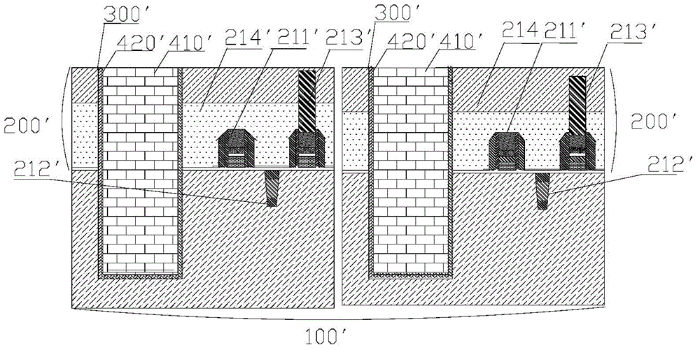
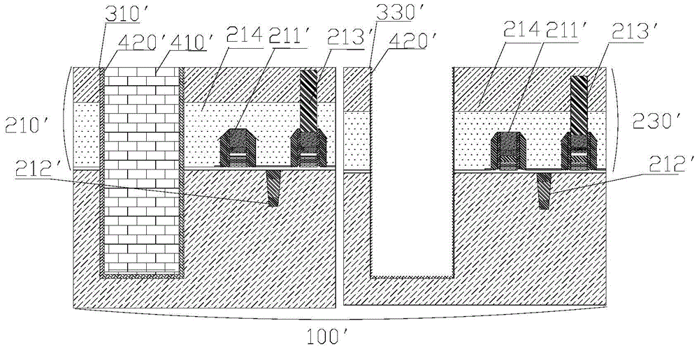
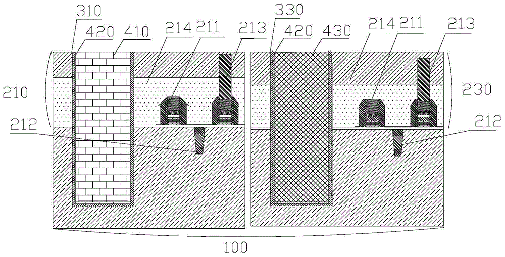
[0034]It can be seen from the background art that in the manufacturing process of the existing chip, there is a problem that the edge washing process will cause the stability of the chip to decrease. The inventor of the present application has conducted a lot of experimental research on the above problems. By chance, the inventor found that after the edge cleaning process removes the conductive layer in the edge penetrating silicon via, the inner wall of the edge penetrating silicon via is directly exposed. , at this time, the barrier layer on the inner wall of the edge TSV is also directly exposed. The exposed barrier layer is easily damaged, cracked, or even peeled off due to the stress gene...
PUM
 Abstract
Description
Claims
Application Information