Touch display substrate and manufacturing method thereof and touch display device

A technology for a touch display substrate and a manufacturing method is applied in the fields of a touch display device, a touch display substrate and a manufacturing method thereof, and can solve the problems of affecting the layout of data lines, poor picture display quality, unbalanced brightness of the display picture, etc. Improve the display effect, enhance the picture display quality, and ensure the effect of brightness

Inactive Publication Date: 2016-12-07
BOE TECH GRP CO LTD +1
View PDF4 Cites 10 Cited by
  • Summary
  • Abstract
  • Description
  • Claims
  • Application Information

AI Technical Summary

Problems solved by technology

However, after the touch signal line is set, since the touch signal line is parallel to the data line, it will affect the layout of the data line. control signal line, the parasitic capacitance Cpd' between the pixel electrode of the sub-pixel in the nth column and the data line n-1 will not be equal to the parasitic capacitance between the pixel electrode of the sub-pixel in the nth column and the nth data line Cpd, due to the coupling effect of parasitic capacitance, the voltage change on the data line will be coupled to the pixel electrode, so that the n-1th data line and the nth data line will be connected to the pixel electrode of the nth column of sub-pixels The influence of different factors is also different, resulting in uneven brightness of the display screen and poor display quality of the screen.

Method used


Image

  • Touch display substrate and manufacturing method thereof and touch display device
  • Touch display substrate and manufacturing method thereof and touch display device
  • Touch display substrate and manufacturing method thereof and touch display device

Examples


Embodiment 1

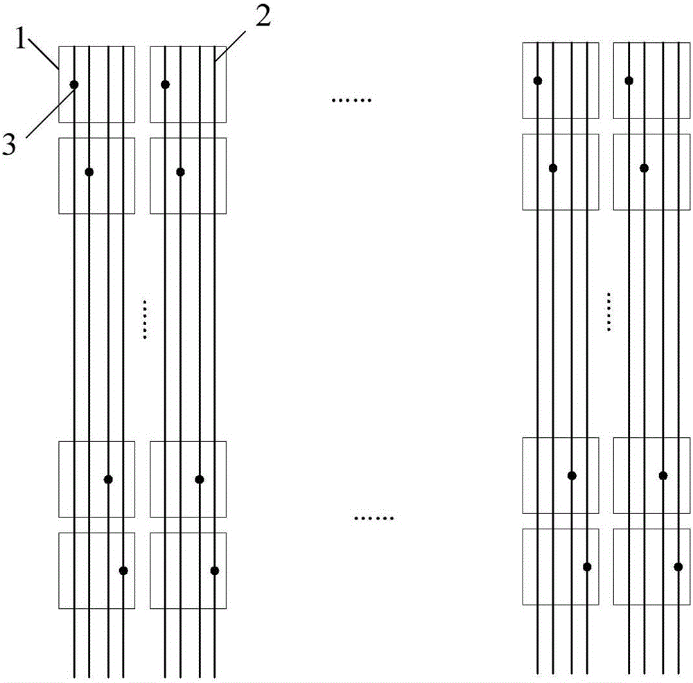
[0038] This embodiment provides a touch display substrate, including a plurality of gate lines and a plurality of data lines arranged crosswise on the base substrate, and the touch display substrate also includes a plurality of touch electrodes and a plurality of touch signals lines, the touch electrodes are used to load common electrode signals and touch scan signals in a time-division manner, each of the touch electrodes is electrically connected to at least one of the touch signal lines, and the touch signal lines are connected to the grid lines parallel.

[0039] In this embodiment, the touch signal line is parallel to the gate line, so that the arrangement of the touch signal line will not affect the layout of the data lines, and the parasitic capacitance between the pixel electrode of the sub-pixel and the adjacent two data lines can be equal. In this way, when the touch display device is working, two adjacent data lines have the same influence on the pixel electrodes of...

Embodiment 2

[0047] This embodiment also provides a touch display device, including the above-mentioned touch display substrate, and also includes a touch chip, each of the touch electrodes is connected to the touch chip through a corresponding touch signal line The touch signal line transmits the touch scanning signal to the touch electrode during the touch stage, and transmits the touch signal generated by the touch electrode at the position where the touch occurs to the touch chip.

[0048] In a specific embodiment, the touch control chip is multiplexed as the gate drive chip of the touch display device, so that one chip can realize the touch control function and output the scanning signal at the same time without increasing the number of chips.

Embodiment 3

[0050] This embodiment provides a method for manufacturing a touch display substrate. The touch display substrate includes a plurality of gate lines and a plurality of data lines arranged crosswise on the base substrate. The touch display substrate further includes a plurality of a touch electrode, the touch electrode is used to time-divisionally load the common electrode signal and the touch scan signal, and the manufacturing method includes:

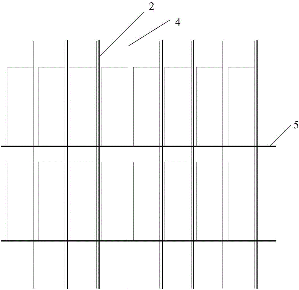
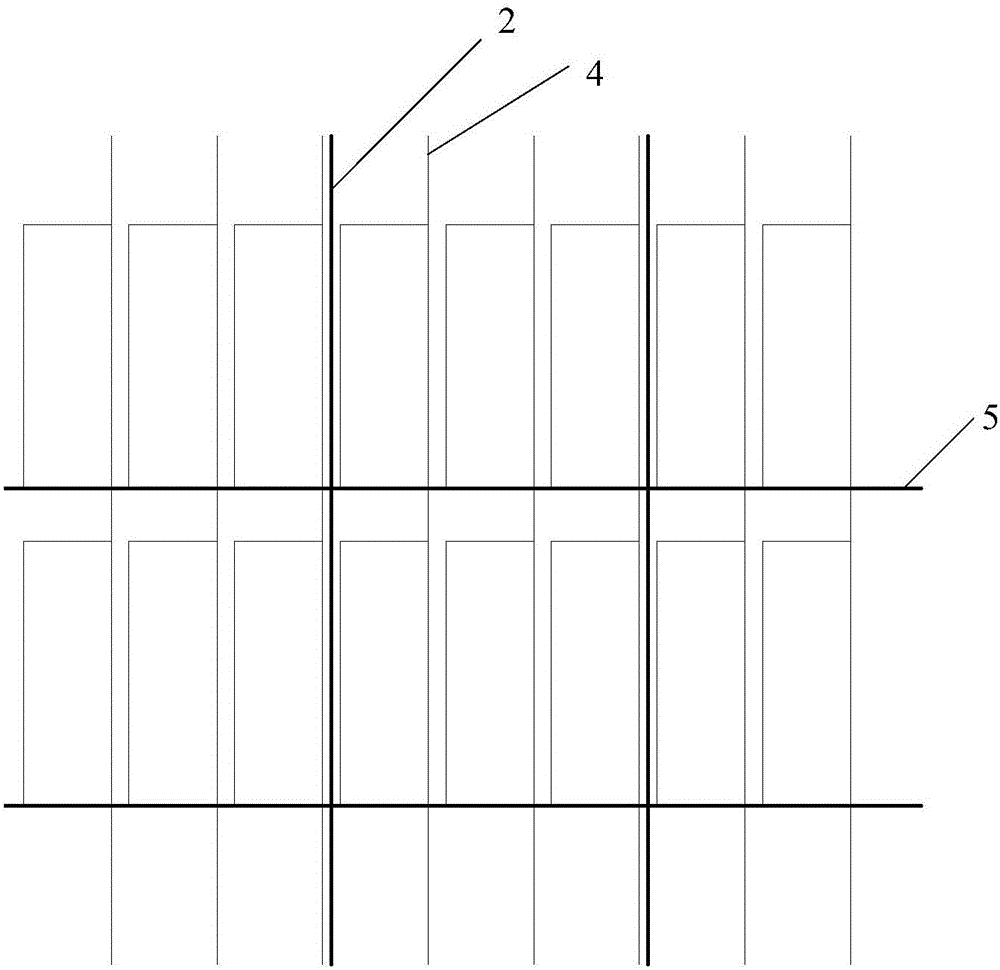
[0051] A plurality of touch signal lines parallel to the gate lines are formed, and each of the touch electrodes is electrically connected to at least one of the touch signal lines.

[0052] In this embodiment, the touch signal lines are made parallel to the gate lines, so that the arrangement of the touch signal lines will not affect the layout of the data lines, and the parasitic connection between the pixel electrode of the sub-pixel and two adjacent data lines can be reduced. The capacitances are equal, so that when the touch displ...


PUM


Abstract

The invention provides a touch display substrate and a manufacturing method thereof and a touch display device, and belongs to the field of touch display. The touch display substrate comprises a plurality of grid lines and a plurality of data lines, the grid lines and the data lines are arranged on an underlayer substrate in a staggered mode, the touch display substrate further comprises a plurality of touch electrodes and a plurality of touch signal lines, the touch electrodes are used for loading public electrode signals and touch scanning signals in a time sharing mode, each touch electrode is electrically connected with at least one touch signal line, and the touch signal lines are parallel to the grid lines. According to the technical scheme, the display effect of the touch display device can be improved, and the picture display quality of the touch display device can be improved.

Description

technical field [0001] The present invention relates to the field of touch display, in particular to a touch display substrate, a manufacturing method thereof, and a touch display device. Background technique [0002] With the development of touch screen technology and market requirements, the thinning of the overall module is the market development trend, so the touch structure is developed from the touch sensor plug-in type to the touch sensor embedded type, so that the thickness of the touch panel can be reduced. At the same time, the cost of the touch screen is greatly reduced. Currently, there are three main types of in-cell touch panels: resistive touch panels, capacitive touch panels, and optical touch panels. [0003] In the prior art, the realization principle of the self-capacitive touch display device is to multiplex the common electrodes into self-capacitive touch electrodes in the touch stage, and each capacitive touch electrode is connected to the touch chip th...

Claims


Application Information

Patent Timeline
Patent Type & Authority Applications(China)
IPC IPC(8): G06F3/044G06F3/041
CPCG06F3/0412G06F3/044G06F2203/04112G06F2203/04103G06F2203/04111G06F3/04166G06F3/0443G06F3/04164
Inventor 王秀娟邵贤杰刘波
Owner BOE TECH GRP CO LTD
Why Eureka
Try Eureka