Formation method for semiconductor structure

A semiconductor and transistor technology, applied in the field of semiconductor structure formation, can solve problems such as poor contact of metal plugs, increased chip manufacturing costs, and difficulty in precise control of polysilicon resistance, and achieves prevention of concave defects, space saving, good height and surface shape. The effect of surface flatness

Active Publication Date: 2016-12-07
SEMICON MFG INT (SHANGHAI) CORP
View PDF6 Cites 9 Cited by
  • Summary
  • Abstract
  • Description
  • Claims
  • Application Information

AI Technical Summary

Problems solved by technology

[0004] Heavily doped polysilicon resistors are widely used in the manufacture of integrated circuits. However, polysilicon resistance is difficult to accurately control, and it needs to be doped specifically for polysilicon, which increases the cost of chip production.
[0005] For this reason, the industry has proposed the use of metal nitride materials to form high-resistance resistors, but the nitride film resistors formed by existing processes have problems such as poor contact with metal plugs.

Method used


Image

  • Formation method for semiconductor structure
  • Formation method for semiconductor structure
  • Formation method for semiconductor structure

Examples


Embodiment Construction

[0030] As mentioned in the background art, the existing metal nitride thin film resistors have the problem of poor contact with the metal plug.

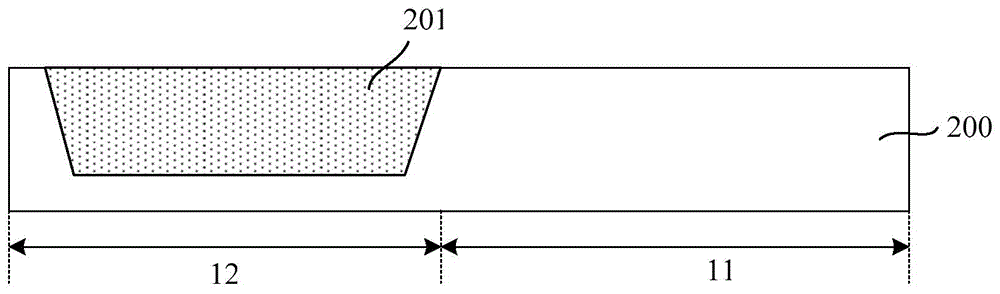
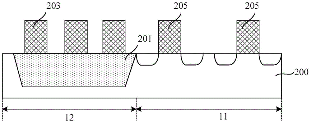
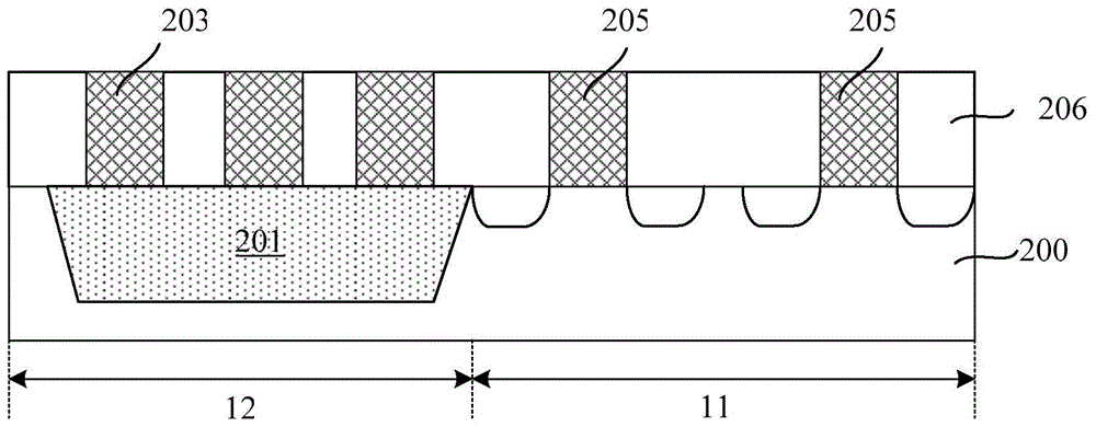
[0031] After research, the formation process of the existing metal nitride thin film resistors is: providing a semiconductor substrate; forming a shallow trench isolation structure in the semiconductor substrate; forming a metal nitride thin film layer on the shallow trench isolation structure , the metal nitride thin film layer is used as a thin film resistor; a dielectric layer covering the shallow trench isolation structure, the semiconductor substrate, and the metal nitride thin film layer is formed; the dielectric layer is etched to form an exposed metal nitride layer on the dielectric layer An opening in a thin film layer; the opening is filled with metal to form a plug. Since the formed metal nitride thin film resistors are generally thin, when the dielectric layer is etched to form an opening, the metal nitride thin film resi...


PUM


Abstract

Disclosed is a formation method for a semiconductor structure. The formation method comprises the steps of providing a semiconductor substrate, wherein the semiconductor substrate comprises one or more first regions and one or more second regions; multiple first pseudo-gage structures are formed on the first regions of the semiconductor substrate; multiple second pseudo-gage structures are formed on the second regions of the semiconductor substrate; forming a first dielectric layer which covers the semiconductor substrate; forming a mask layer which covers the second pseudo-gage structures; removing the first pseudo-gage structures from the first regions to form a groove; forming a metal gate electrode in the groove; forming a thin film resistor which covers the second pseudo-gage structures, wherein a first contact region and a second contact region are arranged at the two ends of the thin film resistor respectively; and the first contact region and the second contact region are correspondingly positioned on one second pseudo-gage structure. By adoption of the formation method, the performance of the formed thin film resistor is improved.

Description

technical field [0001] The invention relates to the field of semiconductor manufacturing, in particular to a method for forming a semiconductor structure. Background technique [0002] Semiconductor integrated circuits are widely used in various electronic products, such as mobile phones, computers, personal game devices, navigation devices, etc. Semiconductor integrated circuits are formed using semiconductor manufacturing processes. For example, multiple transistors, resistors, capacitors and other components are fabricated on a wafer, and the components are combined into a complete electronic circuit according to multi-layer and multi-layer wiring. [0003] Especially in integrated circuits used in analog circuits and high-voltage cables, a large number of resistive elements and transistors are formed on a single chip. In order to reduce the energy consumption of the chip, resistors with high precision and high resistance are widely used. [0004] Heavily doped polysilic...

Claims


Application Information

Patent Timeline
Patent Type & Authority Applications(China)
IPC IPC(8): H01L21/28H01L21/762H01L21/768H01L27/06H01L21/02
Inventor 丁士成
Owner SEMICON MFG INT (SHANGHAI) CORP
Why Eureka
Try Eureka