Low-trigger voltage bidirectional SCR device based on buried layer trigger

A low trigger voltage and device technology, applied in the electronic field, can solve the problems that SCR can't achieve voltage clamping and ESD protection can't be realized.

Active Publication Date: 2016-12-07
UNIV OF ELECTRONICS SCI & TECH OF CHINA
View PDF3 Cites 15 Cited by
  • Summary
  • Abstract
  • Description
  • Claims
  • Application Information

AI Technical Summary

Problems solved by technology

[0007] With the continuous advancement of integrated circuit technology, the gate oxide layer of MOS devices is further thinned, which will cause the gate oxide breakdown voltage B Vox to continue to decrease. The trigger voltage of traditional bidirectional SCR devices that rely on pn junction avalanche breakdown to trigger is much higher. Due to the gate oxide breakdown voltage of the protection circuit, the SCR cannot play the role of voltage clamping and cannot achieve effective ESD protection

Method used


Image

  • Low-trigger voltage bidirectional SCR device based on buried layer trigger
  • Low-trigger voltage bidirectional SCR device based on buried layer trigger
  • Low-trigger voltage bidirectional SCR device based on buried layer trigger

Examples


Embodiment 1

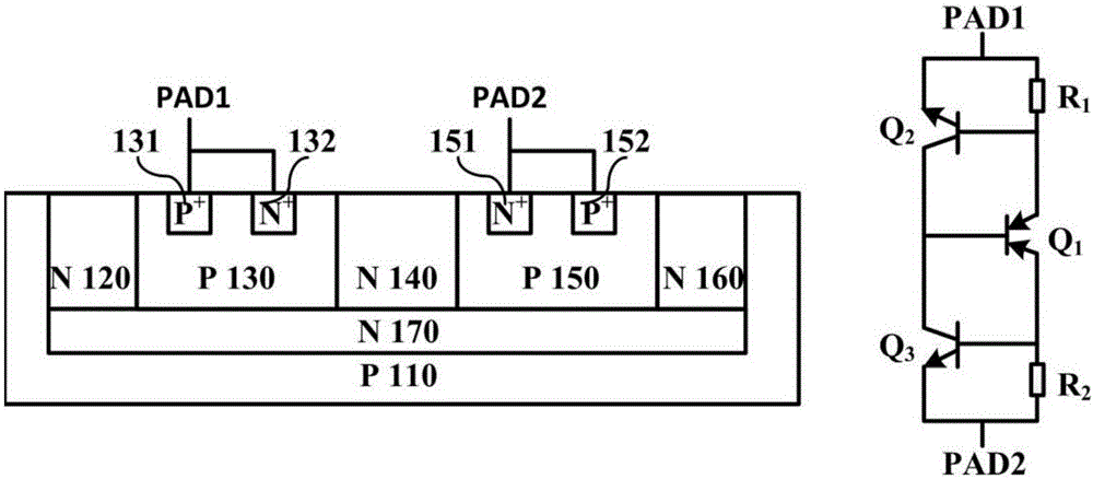
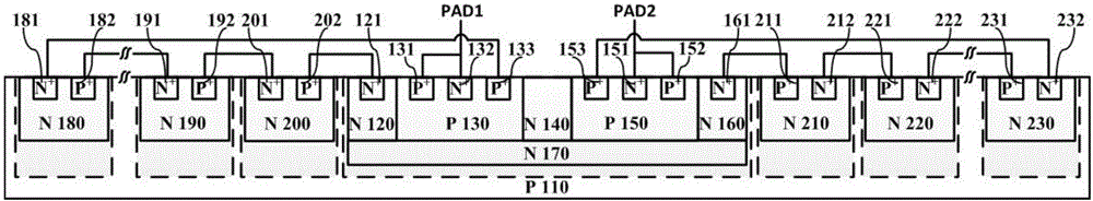
[0021] This embodiment provides a low-trigger voltage bidirectional SCR device based on buried layer triggering, and its structure diagram and equivalent circuit diagram are as follows image 3 As shown, it includes 1 main device, n trigger devices on the left side of the main device, and m trigger devices on the right side of the main device, where n≥1, m≥1;

[0022] The main device has a symmetrical structure and includes a p-type silicon substrate 110; an n-type heavily doped buried layer 170 is formed on the silicon substrate 110; an n-type well is formed on the buried layer 170 adjacent to each other from left to right Region 120, p-type well region 130, n-type well region 140, p-type well region 150, and n-type well region 160; the n-type well region 120 and n-type well region 160 are respectively provided with n-type heavily doped regions 121, 161; The p-type well region 130 is sequentially provided with a p-type heavily doped region 131, an n-type heavily doped region 132,...

Embodiment 2

[0040] This embodiment provides a low-trigger voltage bidirectional SCR device based on buried layer triggering, and its structure diagram and equivalent circuit diagram are as follows Figure 4 As shown, it includes 1 main device, n trigger devices on the left side of the main device, and m trigger devices on the right side of the main device, where n≥1, m≥1; the structure and device of the trigger device on both sides of the main device The connection relationship between them is the same as that of Embodiment 1, and will not be repeated here. The difference is that the p-type well region 130 of the main device is sequentially provided with p-type heavily doped regions 133 and p-type heavily doped regions from left to right. The region 131, the n-type heavily doped region 132, the p-type heavily doped region 131 and the n-type heavily doped region 132 are all connected to the PAD1; the p-type well region 150 is sequentially provided with n-type heavily doped regions from left ...


PUM


Abstract

The invention belongs to the technical field of electronics, and provides a low-trigger voltage bidirectional SCR device based on buried layer trigger for lowering the trigger voltage of the bidirectional SCR device. The bidirectional SCR device is composed of one main device, n trigger devices and m trigger devices at two sides of the main device; the trigger device is a diode device, and the adjacent trigger devices are connected in series; a first conductive type heavily-doped region is respectively arranged in each of the first conductive type well region A and the first conductive type well region C in the bidirectional SCR structure through the main device, a closed first conductive type heavily-doped buried layer only with the isolation effect in the basic bidirectional SCR is connected with the trigger diode strings out of two sides to form a low-voltage trigger channel with the buried layer and the diode strings, thereby lowering the trigger voltage of the bidirectional SCR device; and meanwhile, the trigger voltage is adjustable through the adjustment of the number of the trigger device; the starting speed of the device is effectively improved.

Description

Technical field [0001] The present invention belongs to the field of electronic technology, relates to the design of an electrostatic discharge (ESD: Electro-Static discharge) protection circuit, and specifically relates to a horizontal silicon controlled rectifier SCR (Silicon Controlled Rectifier for short SCR). Background technique [0002] Electro-Static Discharg (ESD for short) refers to the flow of current between two objects with different electrostatic potential energies. Generally speaking, ESD refers to rapid current flow. In people's daily life, ESD phenomenon can be seen everywhere. For integrated circuits, from production to transportation, system integration and user use, all processes may produce electrostatic discharge on the pins of the integrated circuit. The instantaneous large current and high power generated during the ESD process can cause a series of thermal damage to the semiconductor device, which will burn down the semiconductor and metal interconnectio...

Claims


Application Information

Patent Timeline
Patent Type & Authority Applications(China)
IPC IPC(8): H01L27/02
CPCH01L27/0255
Inventor 刘志伟杜飞波刘继芝
Owner UNIV OF ELECTRONICS SCI & TECH OF CHINA
Why Eureka
Try Eureka