Method for reducing injection damage to realize enhanced hemt device and enhanced hemt device

An injection damage and enhancement technology, applied in the field of microelectronics, can solve the problems of etching, small saturation current, affecting the mobility of two-dimensional electron gas, etc., and achieve the effect of simple manufacturing process, large leakage current output, and mature process steps.

Active Publication Date: 2019-03-08
SUZHOU INST OF NANO TECH & NANO BIONICS CHINESE ACEDEMY OF SCI
View PDF4 Cites 0 Cited by
  • Summary
  • Abstract
  • Description
  • Claims
  • Application Information

AI Technical Summary

Problems solved by technology

In order to solve this problem, a recessed gate structure appeared on the basis of the thin barrier layer enhanced HEMT. The recessed gate structure solved the problem of small saturation current, but the barrier layer of a general HEMT device is only 20-30nm, and the etching process is used. The process of forming the concave gate structure is difficult to control and the repeatability is poor
The P-type cap layer does not require an etching process, but an interface state is generated, which affects the stability of the device
F plasma treatment can also realize enhanced HEMT devices, and does not require etching, but in the process of implanting F ions, due to the existence of plasma, the phenomenon of etching barrier layers will occur, and due to the existence of various ions in the plasma , it is difficult to control in the experiment. If the ion implanter is directly used to implant F ions or other ions that can deplete the two-dimensional electron gas into the barrier layer, since the barrier layer is only about 20-30nm, and the general ion implanter The implantation energy is high, so more defects will be generated during ion implantation. When the number of defects reaches a certain amount, the formed defects will form defect rings or other stable structures. It is difficult for semiconductors to recover after high-temperature annealing, which seriously affects the two-dimensional electron gas Mobility, so that the source and drain current of the device is small when the device is turned on

Method used


Image

  • Method for reducing injection damage to realize enhanced hemt device and enhanced hemt device
  • Method for reducing injection damage to realize enhanced hemt device and enhanced hemt device
  • Method for reducing injection damage to realize enhanced hemt device and enhanced hemt device

Examples


Embodiment 1

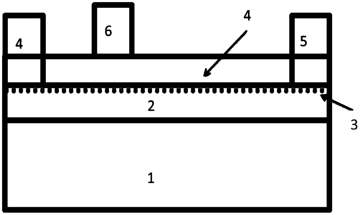
[0067] Embodiment 1 please refer again figure 2 and image 3 , the HEMT has: a first semiconductor 2 (GaN), and a second semiconductor 4 (AlGaN) formed on the first semiconductor 2 . The first semiconductor 2 is not intentionally doped. The second semiconductor 4 may be doped with n-type impurities, or may not be doped. The band gap of the second semiconductor 4 is wider than that of the first semiconductor 2 . The thickness of the second semiconductor 4 is about 15 to 30 nm. The first semiconductor 2 and the second semiconductor 4 form a heterostructure, forming a two-dimensional electron gas (2DEG) at the interface.

[0068] This HEMT has a drain electrode 6 and a source electrode 5 arranged at a distance from each other. The drain electrode 6 and the source electrode 5 extend through the second semiconductor 4 to the first semiconductor 2 and are connected to the two-dimensional electron gas in the channel. The drain electrode 6 and the source electrode 5 are ohmic c...

Embodiment 2

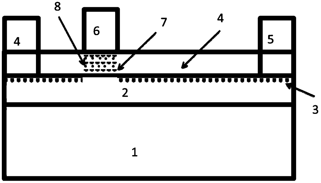
[0071] Embodiment 2 This MIS-HEMT has a first semiconductor 2 (GaN), and a second semiconductor 4 (AlGaN) formed on the first semiconductor 2 . The first semiconductor 2 is not intentionally doped. The second semiconductor 4 may be doped with n-type impurities, or may not be doped. The band gap of the second semiconductor 4 is wider than that of the first semiconductor 2 . The thickness of the second semiconductor 4 is about 15 to 30 nm. The first semiconductor 2 and the second semiconductor 4 form a heterostructure, forming a two-dimensional electron gas (2DEG) at the interface.

[0072]This MIS-HEMT has a drain electrode 6 and a source electrode 5 arranged at predetermined intervals. The drain electrode 6 and the source electrode 5 extend through the second semiconductor 4 to the first semiconductor 2 and are connected to the two-dimensional electron gas in the channel. The drain electrode 6 and the source electrode 5 are made of multi-layer metals (eg Ti / Al / Ti / Au or Ti / ...


PUM


Abstract

The invention discloses a method for reducing implantation damage to realize an enhanced HEMT device, which includes: at least providing a heterostructure mainly composed of a first semiconductor and a second semiconductor, wherein the second semiconductor is formed on the surface of the first semiconductor, and having a band gap wider than that of the first semiconductor, and two-dimensional electron gas is also distributed in the heterostructure; and performing ion implantation on a selected region on the second semiconductor in more than two times to form an ion implantation region, And at least after a selected ion implantation is completed, the device is also annealed to repair the device damage caused by the ion implantation; the ion implantation region is distributed under the gate electrode and above the first semiconductor to deplete Two-dimensional electron gas under the grid. The invention also discloses an enhanced HEMT device. The invention can effectively realize the enhanced HEMT device, and the threshold voltage of the device can be adjusted through the implanted ion dose, the manufacturing process is simple, the repeatability is good, and it is suitable for industrial production.

Description

technical field [0001] The invention relates to a method for manufacturing an enhanced HEMT (high electron mobility transistor) device, in particular to a method for reducing injection damage to realize a high-performance enhanced HEMT device (such as a group III nitride enhanced HEMT device), belonging to field of microelectronics technology. Background technique [0002] HEMT devices are made by making full use of the two-dimensional electron gas formed by the heterojunction structure of semiconductors. Compared with HEMTs made of other materials (such as AlGaAs / GaAs), group III nitride semiconductors are due to piezoelectric polarization and spontaneous The polarization effect, on the AlGaN / GaN heterostructure (Heterostructure), can form a high concentration of two-dimensional electron gas. Therefore, in HEMT devices made of AlGaN / GaN heterojunction, the barrier layer AlGaN generally does not need to be doped. In addition, group III nitrides have the characteristics of ...

Claims


Application Information

Patent Timeline
Patent Type & Authority Patents(China)
IPC IPC(8): H01L29/66H01L21/265H01L21/266H01L29/06H01L29/778
Inventor 于国浩张志利蔡勇张宝顺付凯孙世闯宋亮
Owner SUZHOU INST OF NANO TECH & NANO BIONICS CHINESE ACEDEMY OF SCI
Why Eureka
Try Eureka