Group III nitride enhanced hemt device and manufacturing method thereof

A manufacturing method and nitride technology, which are applied in the field of microelectronics, can solve the problems affecting the mobility of two-dimensional electron gas, small source-leakage current, and etching barrier layers, so as to achieve mature process steps, less mobility reduction, and The effect of simple process

Active Publication Date: 2020-05-19
SUZHOU INST OF NANO TECH & NANO BIONICS CHINESE ACEDEMY OF SCI
View PDF5 Cites 0 Cited by
  • Summary
  • Abstract
  • Description
  • Claims
  • Application Information

AI Technical Summary

Problems solved by technology

In order to solve this problem, a recessed gate structure appeared on the basis of the thin barrier layer enhanced HEMT. The recessed gate structure solved the problem of small saturation current, but the barrier layer in a general HEMT device is only 20-30nm. It is difficult to control the process of forming the concave gate structure by etching process, and the repeatability is poor
The P-type cap layer does not require an etching process, but an interface state is generated, which affects the stability of the device
F plasma treatment can also realize enhanced HEMT devices, and does not require etching, but in the process of implanting F ions, due to the existence of plasma, the phenomenon of etching barrier layers will occur, and due to the existence of various ions in the plasma , it is difficult to control in the experiment. If the ion implanter is directly used to implant F ions into the barrier layer, since the barrier layer is only about 20-30nm, and the implantation energy of the general ion implanter is relatively high, the implanted F ions pass through The barrier layer AlGaN enters the GaN buffer layer, which seriously affects the mobility of the two-dimensional electron gas, so that the source-drain current of the device is small when the device is turned on.

Method used


Image

  • Group III nitride enhanced hemt device and manufacturing method thereof
  • Group III nitride enhanced hemt device and manufacturing method thereof
  • Group III nitride enhanced hemt device and manufacturing method thereof

Examples


Embodiment 1

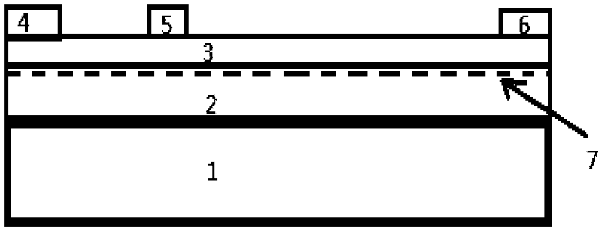
[0072] Embodiment 1 please refer again image 3 with Figure 4 , the HEMT has: a first semiconductor 2 (GaN), and a second semiconductor 3 (AlGaN) formed on the first semiconductor 2 . The first semiconductor 2 is not intentionally doped. The second semiconductor 3 may be doped with n-type impurities, or may not be doped. The band gap of the second semiconductor 3 is wider than that of the first semiconductor 2 . The thickness of the second semiconductor 3 is about 15 to 30 nm. The first semiconductor 2 and the second semiconductor 3 form a heterostructure, forming a two-dimensional electron gas (2DEG) at the interface.

[0073] This HEMT has a drain electrode 6 and a source electrode 4 arranged at a distance apart. The drain electrode 6 and the source electrode 4 extend through the second semiconductor 3 to the first semiconductor 2 and are connected to the two-dimensional electron gas in the channel. The drain electrode 6 and the source electrode 4 are made of multilay...

Embodiment 2

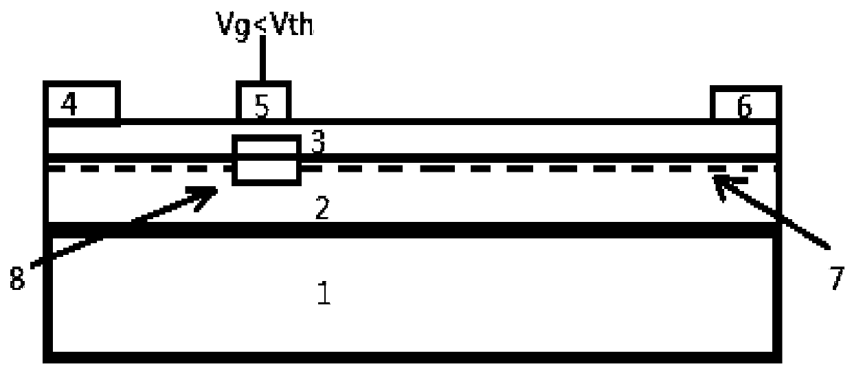
[0077] Embodiment 2 This MIS-HEMT has: a first semiconductor 2 (GaN), and a second semiconductor 3 (AlGaN) formed on the first semiconductor 2 . The first semiconductor 2 is not intentionally doped. The second semiconductor 3 may be doped with n-type impurities, or may not be doped. The band gap of the second semiconductor 3 is wider than that of the first semiconductor 2 . The thickness of the second semiconductor 3 is about 15 to 30 nm. The first semiconductor 2 and the second semiconductor 3 form a heterostructure, forming a two-dimensional electron gas (2DEG) at the interface.

[0078]This MIS-HEMT has a drain electrode 6 and a source electrode 4 arranged at predetermined intervals. The drain electrode 6 and the source electrode 4 extend through the second semiconductor 3 to the first semiconductor 2, and are connected to the two-dimensional electron gas in the channel. The drain electrode 6 and the source electrode 4 are made of multilayer metals (such as: Ti / Al / Ti / Au...


PUM

PropertyMeasurementUnit
thicknessaaaaaaaaaa
thicknessaaaaaaaaaa
thicknessaaaaaaaaaa

Abstract

The invention discloses a Group III nitride enhanced HEMT device and a manufacturing method thereof. The device includes source, drain, gate electrodes and a heterostructure. The source and drain electrodes are electrically connected through the two-dimensional electron gas formed in the heterostructure. The heterostructure includes first and second semiconductors, and the second semiconductor has a width wider than The band gap of the first semiconductor, the first semiconductor is arranged between the source and drain electrodes, the gate electrode is arranged on the surface of the second semiconductor, the second semiconductor also contains a P-type doped region, and the P-type doped region is distributed under the gate electrode However, above the first semiconductor, the gate electrode includes: a first gate electrode material layer that forms a Schottky contact with the second semiconductor and serves as an ion implantation energy absorption layer, and a second gate electrode material layer stacked on the first gate electrode material layer. gate electrode material layer. The invention can effectively realize the enhanced HEMT device, and the threshold voltage of the device can be adjusted through the implanted ion dose, the manufacturing process is simple, the repeatability is good, and it is suitable for industrial production.

Description

technical field [0001] The invention relates to a Group III nitride enhanced HEMT device and a manufacturing method thereof, in particular to a method for realizing enhanced GaN HEMT by ion implantation, which belongs to the field of microelectronics technology. Background technique [0002] HEMT devices (High Electron Mobility Transistors) are made by making full use of the two-dimensional electron gas formed by the heterojunction structure of semiconductors. Compared with HEMTs made of other materials (such as AlGaAs / GaAs), Group III nitride semiconductors Due to the piezoelectric polarization and spontaneous polarization effects, a high-concentration two-dimensional electron gas can be formed on the AlGaN / GaN heterostructure (Heterostructure). Therefore, in HEMT devices made of AlGaN / GaN heterojunction, the barrier layer AlGaN generally does not need to be doped. In addition, group III nitrides have the characteristics of large band gap, high saturated electron drift vel...

Claims


Application Information

Patent Timeline
Patent Type & Authority Patents(China)
IPC IPC(8): H01L29/778H01L29/06H01L29/423H01L21/335H01L21/28H01L21/265
CPCH01L21/26546H01L29/0684H01L29/42376H01L29/66462H01L29/7787
Inventor 张志利蔡勇张宝顺付凯于国浩孙世闯宋亮
Owner SUZHOU INST OF NANO TECH & NANO BIONICS CHINESE ACEDEMY OF SCI
Why Eureka
Try Eureka