Metal insulated semi-conductor (MIS) grid GaN base enhancing high electro mobility transistor (HEMT) device and manufacture method

An enhanced device technology, applied in the field of microelectronics, can solve the problems of poor threshold voltage regulation, influence of device performance and reliability, low repeatability, etc., and achieve the effects of good regulation, good enhanced characteristics, and high threshold voltage.

Inactive Publication Date: 2012-08-22
XIDIAN UNIV
View PDF4 Cites 11 Cited by
  • Summary
  • Abstract
  • Description
  • Claims
  • Application Information

AI Technical Summary

Problems solved by technology

[0012] First, there is a trade-off relationship between threshold voltage and current density, and it is difficult to achieve coexistence of high threshold voltage and high current density, and the regulation of threshold voltage is poor;
[0013] Second, whether etching to form trench gates or fluorine ion implantation will cause damage to the material, although a certain amount of damage can be eliminated after annealing, the remaining damage will still affect device performance and reliability. At the same time, the repeatability of this process is still low. not tall;
[0014] Third, when forming short-channel devices for microwave applications, it is necessary to use high-end process equipment such as electron beam direct writing to produce short gate lengths, and the process is relatively difficult.

Method used


Image

  • Metal insulated semi-conductor (MIS) grid GaN base enhancing high electro mobility transistor (HEMT) device and manufacture method
  • Metal insulated semi-conductor (MIS) grid GaN base enhancing high electro mobility transistor (HEMT) device and manufacture method
  • Metal insulated semi-conductor (MIS) grid GaN base enhancing high electro mobility transistor (HEMT) device and manufacture method

Examples


Embodiment 1

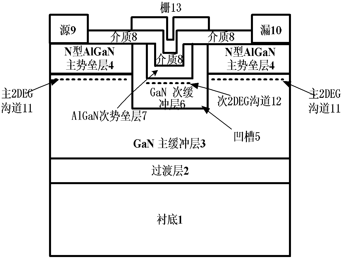
[0049] The transition layer is made of AlN, the thickness of the GaN main buffer layer is 1um, and the thickness of the Al 0.35 Ga 0.65 The thickness of the N main barrier layer is 14nm, and the groove etching depth is 35nm. 0.35 Ga 0.65 The N-time barrier layer is an MIS gate GaN-based enhanced HEMT device with a thickness of 14nm in the upward direction of the bottom of the groove, a thickness of 7nm in the horizontal direction of the groove side, and a gate dielectric layer of 20nm. The steps are:

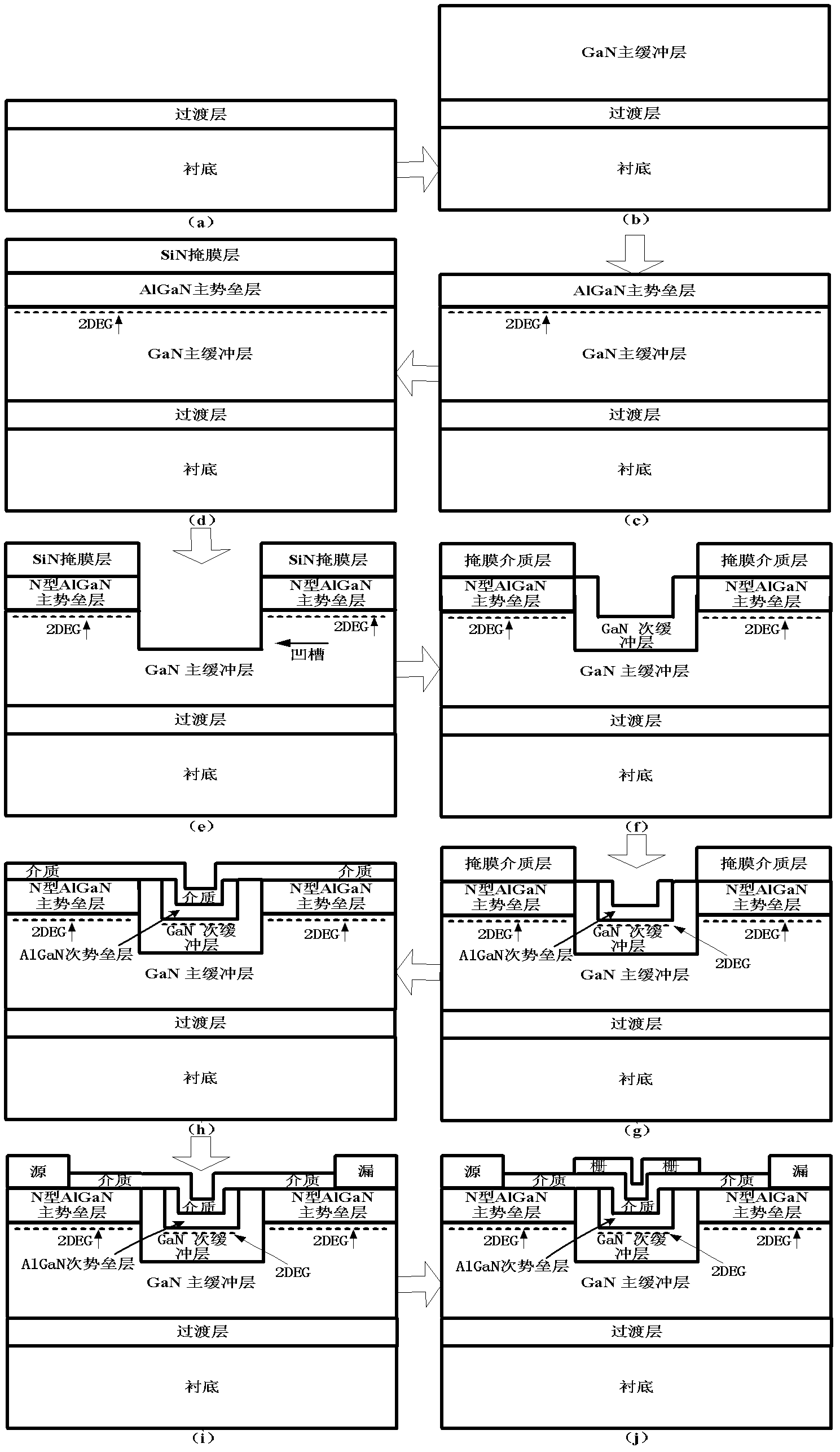
[0050] Step 1, place the C-plane sapphire substrate in the reaction chamber of the MOCVD equipment, and evacuate the vacuum of the reaction chamber to 1×10 -2 Under Torr, the sapphire substrate is heat-treated and surface nitrided under the protection of a mixed gas of hydrogen and ammonia. The heating temperature is 1050°C, the pressure is 20Torr, the flow rate of hydrogen gas is 1500 sccm, and the flow rate of ammonia gas is 1500 sccm.

[0051] Step 2, using MOCVD technolog...

Embodiment 2

[0082] The transition layer is made of AlN, the thickness of the GaN main buffer layer is 2um, and the thickness of the Al 0.27 Ga 0.73 The thickness of the N main barrier layer is 24nm, and the groove etching depth is 80nm. 0.27 Ga 0.73 The N-time barrier layer is an MIS gate GaN-based enhanced HEMT device with a thickness of 24nm in the upward direction on the bottom of the groove, a thickness of 12nm in the horizontal direction on the side of the groove, and a gate dielectric layer thickness of 40nm. The steps are:

[0083] Step 1 is the same as Step 1 of Embodiment 1.

[0084] Step 2 is the same as Step 2 of Example 1.

[0085] Step 3, using MOCVD technology to epitaxially grow a GaN main buffer layer with a thickness of 2um on the transition layer, such as figure 2 (b).

[0086] The process conditions adopted for the epitaxy are: the temperature is 920° C., the pressure is 40 Torr, the flow rate of hydrogen gas is 500 sccm, the flow rate of ammonia gas is 5000 sccm,...

Embodiment 3

[0110] The transition layer is made of AlN, the thickness of the GaN main buffer layer is 3um, and the thickness of the Al 0.2 Ga 0.8 The thickness of the N main barrier layer is 30nm, the etching depth of the groove is 140nm, the thickness of the GaN sub-buffer layer is 100nm in the upward direction of the bottom of the groove, and 50nm in the horizontal direction of the side of the groove. 0.2 Ga 0.8 The N-time barrier layer is an MIS gate GaN-based enhanced HEMT device with a thickness of 30nm in the upward direction on the bottom of the groove, a thickness of 15nm in the horizontal direction on the side of the groove, and a gate dielectric layer thickness of 60nm. The steps are:

[0111] Step A is the same as step one of embodiment 1.

[0112] Step B is the same as Step 2 of Example 1.

[0113] Step C, using MOCVD technology to epitaxially grow a GaN main buffer layer with a thickness of 3um on the transition layer, such as figure 2 (b).

[0114] The process conditio...


PUM


Abstract

The invention discloses a metal insulated semi-conductor (MIS) grid GaN base enhancing high electro mobility transistor (HEMT) device and a manufacture method, which mainly solve the problems that the existing GaN base enhancing device is low in threshold voltage, poor in controllability and low in reliability. The device comprises a substrate (1), a transition layer (2), a GaN main buffering layer (3) and an N-type AlGaN main barrier layer (4). A source (9) and a drain (10) are arranged on two sides of the top end of the N-type AlGaN main barrier layer (4), a grid (13) is arranged in the middle of the top end of the source (9) and the drain (10), a groove (5) is etched in the middle of the GaN main buffering layer (3), the bottom of the groove is a 0001 polarity plane, a lateral side of the groove is a non-0001 plane, and an inner wall of the groove extends outwards to form a GaN auxiliary buffering layer (6), a AlGaN auxiliary barrier layer (7) and a medium layer (8). The grid (13) is deposited on the medium layer (8). The MIS grid GaN base enhancing HEMT device and the manufacture method have the advantages of being high in threshold voltage, good in regulation performance, high in current density, good in pinching-off performance, simple and mature in manufacture process and good in repeatability and can be used for high temperature high power application situations and digital circuits.

Description

technical field [0001] The invention belongs to the technical field of microelectronics and relates to a semiconductor device, in particular to an MIS gate GaN-based enhanced HEMT device and a manufacturing method, which can be used in high-temperature and high-power applications and form basic units of digital circuits. Background technique [0002] With the development of modern weaponry and aerospace, nuclear energy, communication technology, automotive electronics, and switching power supplies, higher requirements are placed on the performance of semiconductor devices. As a typical representative of wide bandgap semiconductor materials, GaN-based materials have the characteristics of large bandgap width, high electron saturation drift velocity, high critical breakdown field strength, high thermal conductivity, good stability, corrosion resistance, and radiation resistance. Used in the production of high temperature, high frequency and high power electronic devices. In a...

Claims


Application Information

Patent Timeline
Patent Type & Authority Applications(China)
IPC IPC(8): H01L29/778H01L29/04H01L21/335
Inventor 张进成张琳霞郝跃王冲马晓华党李莎鲁明周昊孟凡娜侯耀伟姜腾
Owner XIDIAN UNIV
Why Eureka
Try Eureka