An optically written non-volatile magnetic memory

A magnetic memory and non-volatile technology, applied in the field of non-volatile memory, can solve the problems of high write delay, high current, increased manufacturing and processing costs, etc., to reduce energy consumption and delay, and reduce power consumption , The effect of reducing the tunneling current

Active Publication Date: 2018-08-28
BEIHANG UNIV
View PDF6 Cites 0 Cited by
  • Summary
  • Abstract
  • Description
  • Claims
  • Application Information

AI Technical Summary

Problems solved by technology

[0004] 1. For electrical writing and electrical reading of rotational transfer torque magnetic random access memory, since the process of reading data and writing data uses current, in order to avoid confusion between reading and writing, the writing current is much larger than the reading current. take current, which results in high write power consumption
For magnetic write and electrical read resistive magnetic random access memory, the rapid reversal of the magnetic field requires a large current, and the power consumption problem is also very significant.
[0005] 2. Regardless of whether it is written by current or magnetic field, it has a high write delay. Therefore, the current write rate of non-volatile memory is greatly limited and cannot be used for high-speed computing.
[0006] 3. With the continuous reduction of the size of the manufacturing process, the deviation of the process parameters is increasing, and the reliability of STT-RAM is reduced, especially when entering the deep submicron process line (for example, less than 40nm), its bit error rate (Bit Error Rate , BER) getting higher and higher
[0007] 4. The magnetic writing method of changing the magnetization of the free layer by changing the external magnetic field restricts the miniaturization of the storage unit, which is not conducive to large-scale integration, and significantly increases the manufacturing and processing costs

Method used


Image

  • An optically written non-volatile magnetic memory
  • An optically written non-volatile magnetic memory
  • An optically written non-volatile magnetic memory

Examples


Embodiment Construction

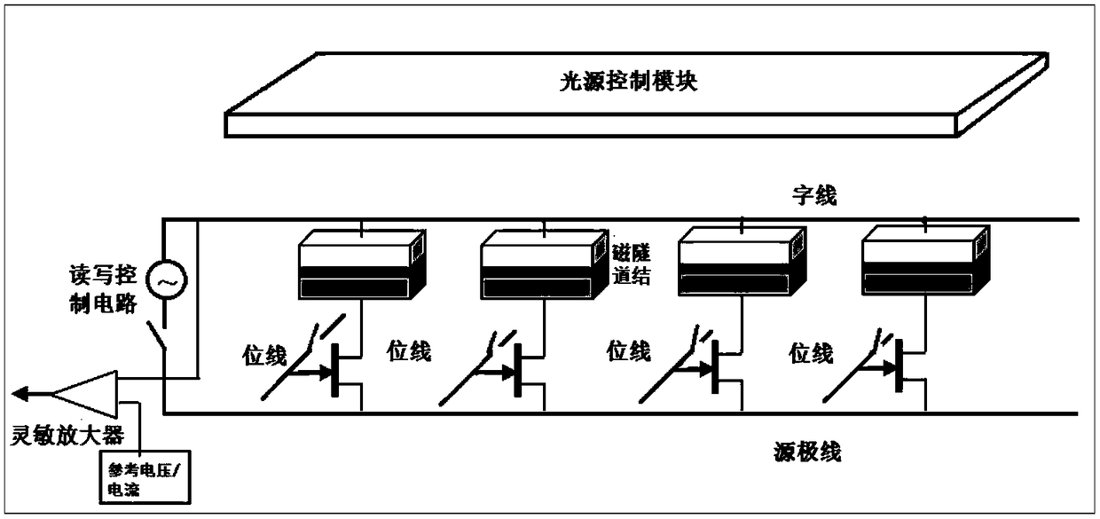
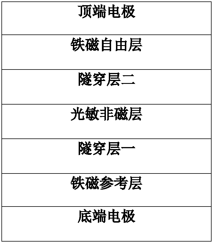
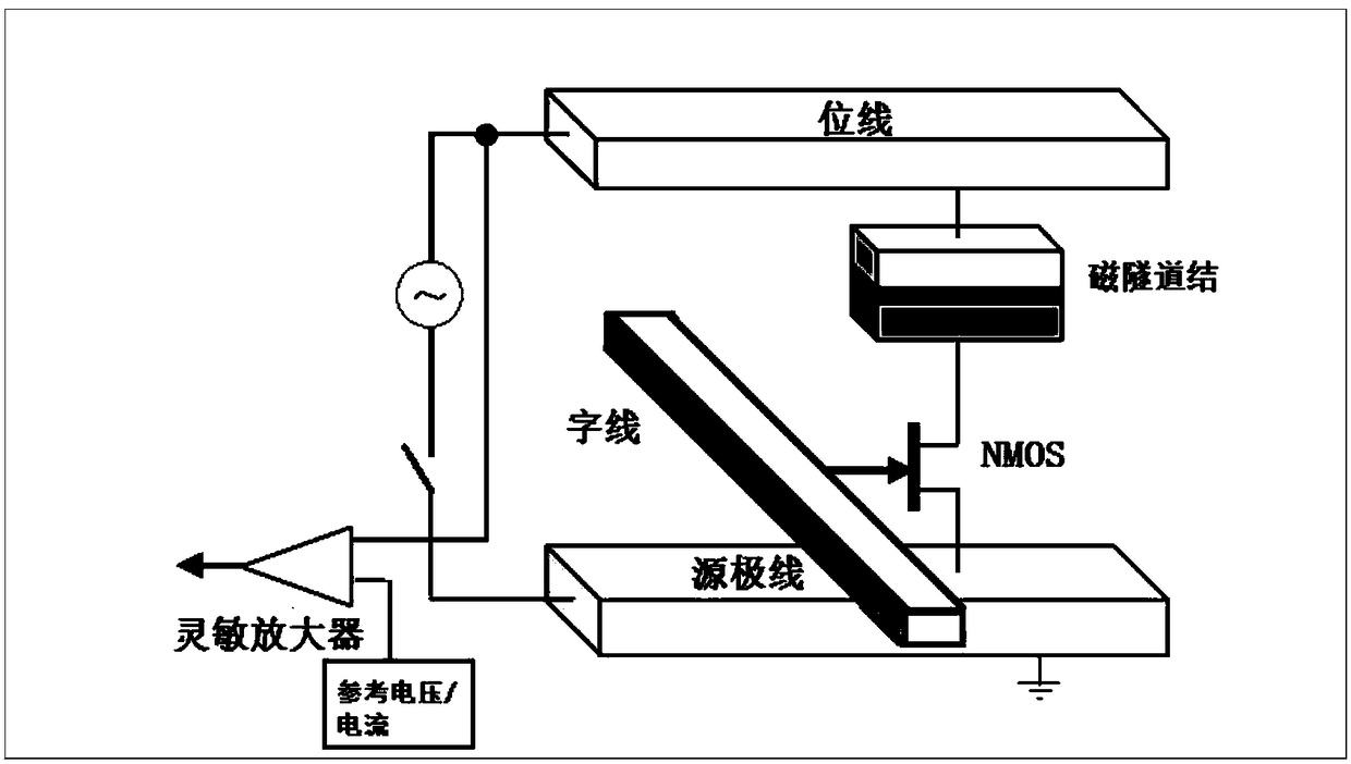
[0035] The invention proposes an optically written nonvolatile memory, which has the characteristics of fast writing speed, low writing power consumption and non-volatile by realizing the optical writing of storage state.

[0036] The substantive features of the present invention are further described with reference to the accompanying drawings. The drawings are all schematic diagrams, and the thicknesses of the functional layers or regions involved are not actual dimensions, and the resistance and voltage values ​​in the working mode are also not actual values.

[0037] Detailed exemplary embodiments are disclosed herein, specific structural and functional details are merely representative for purposes of describing exemplary embodiments, therefore, the invention may be embodied in many alternative forms and should not be construed as It is to be construed as being limited only to the exemplary embodiments set forth herein, but to cover all changes, equivalents, and alternative...


PUM


Abstract

The invention relates to a light-induced nonvolatile magnetic memory which is composed of a light source control module, magnetic tunnel junctions and a reading-writing control circuit. The light source control module is composed of word lines, bit lines and light source dot matrixes, the dot matrixes correspond to magnetic tunnel junction arrays in one to one mode, the state of any point light source of any dot matrix can be controlled through the word lines and the bit lines, and writing in of a single magnetic tunnel junction storage state is completed. The reading-writing control circuit is composed of word lines, bit lines, a transistor, a sensible amplifier and an accessory circuit and performs gating and reading-writing control of a storage unit. Each magnetic tunnel junction comprises a bottom-end electrode, a ferromagnetic reference layer, a tunneling layer I, a photosensitive non-magnetic layer, a tunneling layer II, a ferromagnetic free layer and a top-end electrode which are sequentially and vertically stacked from bottom to top, wherein the ferromagnetic free layer and the ferromagnetic reference layer are changeable in position. The light-induced nonvolatile magnetic memory can achieve data light writing in, reduces tunneling current and power consumption, has nonvolatile properties, reduces the power consumption and delay in the writing in process and reduces the bit error rate while facilitating device miniaturization.

Description

【Technical field】 [0001] The invention relates to an optically written nonvolatile magnetic memory, which is used for realizing optically written and electrical reading of a storage state, and belongs to the field of nonvolatile memory. 【Background technique】 [0002] In recent years, emerging non-volatile memory technologies, such as Spin Transfer Torque Magnetic Random Access Memory (STT-MRAM), Resistive Random Access Memory (RRAM), and Phase change random access memory (Phase Change Random Access Memory, PCRAM) and the like continue to develop, are receiving more and more attention and are beginning to replace the traditional memory industry. Non-volatile memories have many unique advantages: they can not only keep the stored data from being lost after power failure, but also have higher storage density, do not need to be constantly refreshed to save the stored data, and have smaller leakage currents. Among them, spin-transfer torque magnetic random access memory (STT-MR...

Claims


Application Information

Patent Timeline
Patent Type & Authority Patents(China)
IPC IPC(8): G11C11/16
CPCG11C11/1659
Inventor 赵巍胜林晓阳郑明阳斯志仲孙艳明江雷
Owner BEIHANG UNIV
Why Eureka
Try Eureka