Array substrate and manufacturing method thereof

A technology of an array substrate and a manufacturing method, which is applied in the field of liquid crystal display and can solve the problems of increasing the contact resistance of FOGPad and FPC and affecting the display, etc.

Active Publication Date: 2016-12-14
WUHAN CHINA STAR OPTOELECTRONICS TECH CO LTD
View PDF10 Cites 8 Cited by
  • Summary
  • Abstract
  • Description
  • Claims
  • Application Information

AI Technical Summary

Problems solved by technology

When the resolution corresponding to the panel increases, the number of FOG Pads will increase. In the same space, when the number of FOG Pads increases, the size (length, width) of the FOG Pads will de

Method used


Image

  • Array substrate and manufacturing method thereof
  • Array substrate and manufacturing method thereof
  • Array substrate and manufacturing method thereof

Examples


Embodiment Construction

[0022] The specific implementation of the array substrate provided by the present invention and the manufacturing method thereof will be described in detail below with reference to the accompanying drawings.

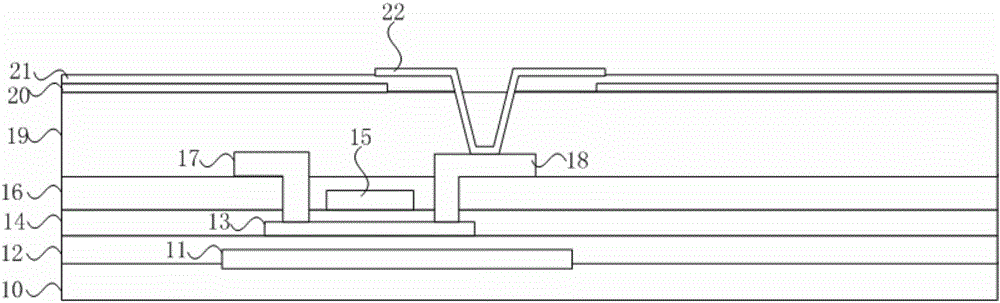
[0023] The array substrate of the present invention includes a display area and a driving area. Since the structure that needs to be explained in the present invention is not in the display area, the display area is not shown in the accompanying drawings. The structure of the display area of ​​the array substrate can be found in figure 1 .

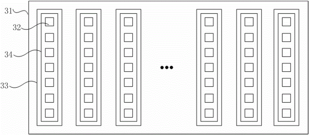
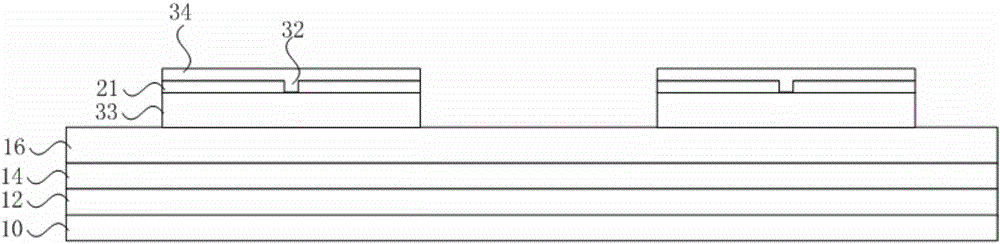
[0024] see Figure 4 and Figure 5 , the driving area includes a pad area 40 having a plurality of pads 41, and the pads 41 are used for electrical connection with an external flexible circuit board (not shown in the drawings). The pad area 40 includes a glass substrate 42, a first insulating layer 43, a second insulating layer 44, and a third insulating layer 45 arranged sequentially from bottom to top, and the solder pads are ar...


PUM


Abstract

The invention provides an array substrate and manufacturing method thereof The array substrate comprises a display area and a driving area, wherein the driving area comprises a pad area having a plurality of pads electrically connected with an external flexible circuit board. The array substrate is characterized in that the pad area comprises a glass substrate, a first insulating layer, a second insulating layer and a third insulating layer, which are arranged from bottom to top sequentially, wherein all pads are arranged on the surface of the third insulating layer, and the second insulating layer and the third insulating layer are each provided with a through hole on the area between two adjacent pads. Section display is increased greatly, attaching area of ACF glue in a limited space is increased, and the adhesion capability of ACF is improved. FOG and FPC contact impedance is reduced, the compression scope of conductive ion in ACF glue becomes large, the compression ratio is increased, and the FOG and FPC contact impedance is reduced.

Description

technical field [0001] The invention relates to the field of liquid crystal display, in particular to an array substrate and a manufacturing method thereof. Background technique [0002] Since LTPS has the advantage of high mobility, the W / L of the TFT switch can be designed to be very small when designing the pixel, so that the aperture ratio corresponding to the pixel is relatively high, which has a great market competitive advantage. Traditional LTPS pixel cross section see figure 1 ,From figure 1 It can be seen that, on the glass substrate 10, a light-shielding layer (LSM) 11, a first insulating layer 12, a polysilicon layer 13, a second insulating layer 14, a gate layer 15, a third insulating layer 16, and a source 17 are sequentially arranged. , a drain electrode 18 , an organic flat layer 19 , a common electrode layer 20 , a passivation layer 21 and a pixel electrode layer 22 . It can be seen that there are many layers of LTPS, and 11 layers are commonly used at pr...

Claims


Application Information

Patent Timeline
IPC IPC(8): H01L23/498H01L27/12H01L21/84H01L21/48
CPCH01L27/124H01L21/4853H01L23/49811H01L23/49844H01L27/1259
Inventor 李亚锋
Owner WUHAN CHINA STAR OPTOELECTRONICS TECH CO LTD
Why Eureka
Try Eureka