
Electrolytic degreasing device for chip type medium and high power semiconductor element lead frame

A technology for component lead and electrolysis degreasing, applied in electrolysis components, electrolysis process, etc., can solve the problems of poor degreasing effect, inconvenient connection of stamped bare copper plates, and inability to completely remove oil stains, and achieves convenient connection and good degreasing effect. Effect

Active Publication Date: 2019-02-05
NINGBO KANGQIANG ELECTRONICS CO LTD
View PDF6 Cites 0 Cited by
  • Summary
  • Abstract
  • Description
  • Claims
  • Application Information

AI Technical Summary

Problems solved by technology

In the manufacturing process of the lead frame of medium and high-power semiconductor components, it is necessary to electrolytically degrease the stamped bare copper plate. At present, there is a device for electrolytic degreasing of the stamped bare copper plate in rolls, but this type of degreasing device generally The stamped bare copper plate is placed statically in the degreasing tank filled with lye, so when it is applied to the sheet-type stamped screw copper plate, on the one hand, the connection between the sheet-type stamped bare copper plate and the electrode is very inconvenient. Type stamped bare copper plates may overlap each other when placed in the degreasing tank, resulting in the inability to completely remove the oil on the surface, and the degreasing effect is poor. Therefore, it is urgent to design an electrolytic degreasing specially for the lead frame of chip-type medium and high-power semiconductor components. device

Method used


Image

  • Electrolytic degreasing device for chip type medium and high power semiconductor element lead frame
  • Electrolytic degreasing device for chip type medium and high power semiconductor element lead frame
  • Electrolytic degreasing device for chip type medium and high power semiconductor element lead frame

Examples


Embodiment

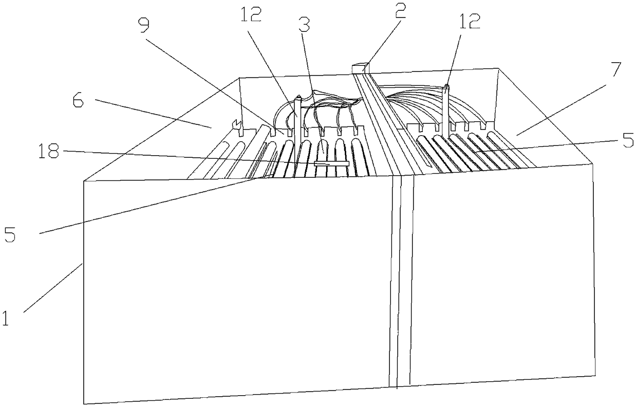
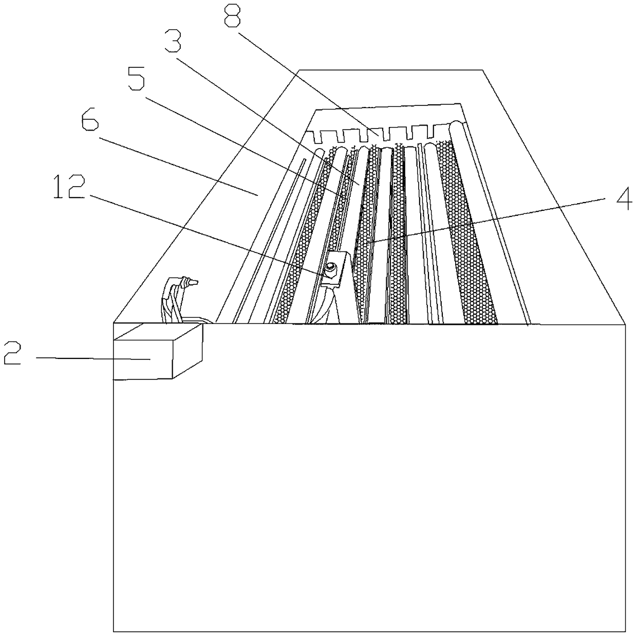
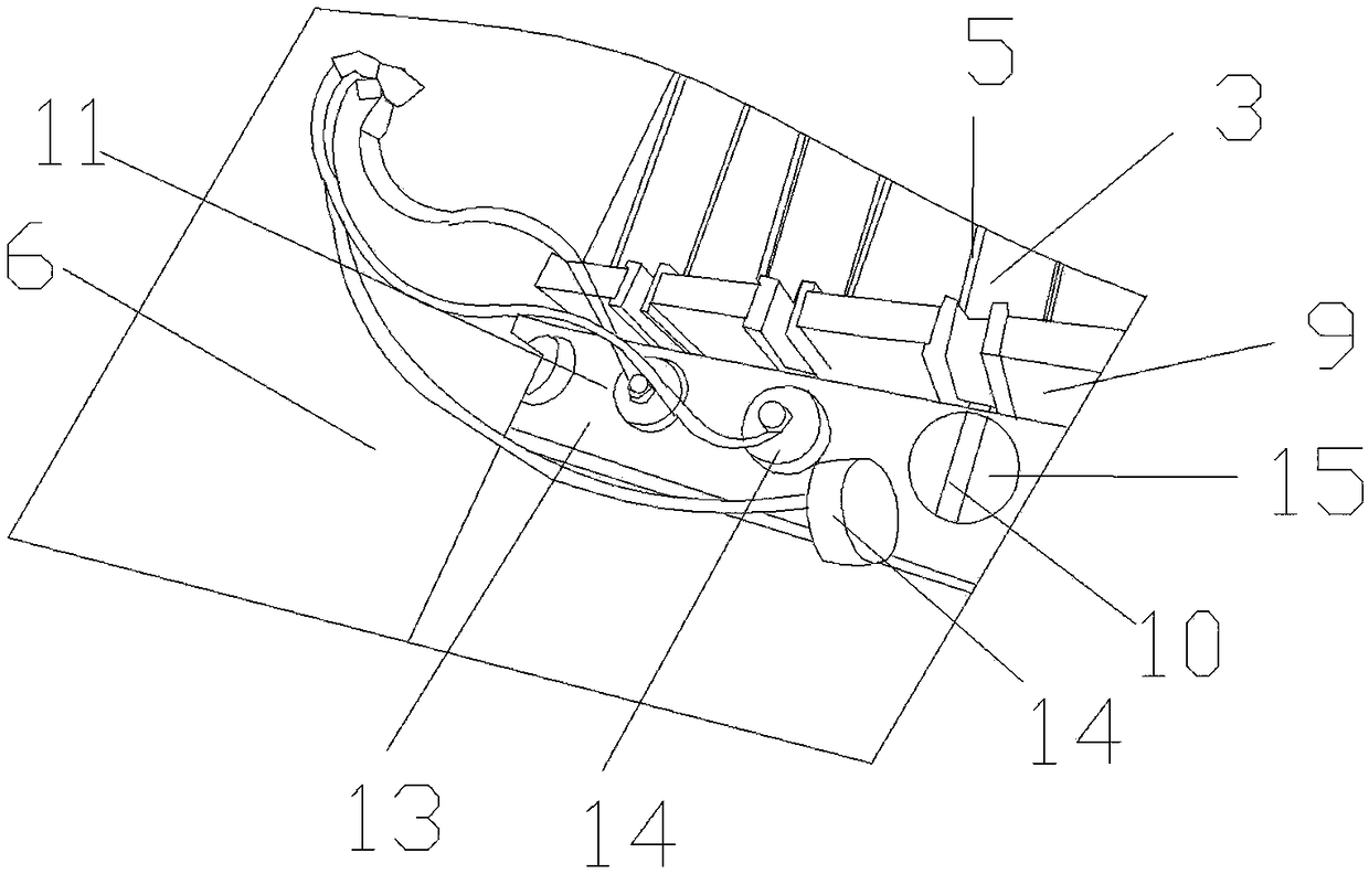
[0020] Such as figure 1 , figure 2 , image 3 As shown, an electrolytic degreasing device for chip-type medium and high-power semiconductor element lead frames includes a degreasing tank 1 and a rectifier 2, and is characterized in that: it also includes a chip type that is arranged side by side on the upper part of the degreasing tank 1 for transmission and electrical connection. A plurality of conductive rollers 3 of the bare copper plate 18 and a conductive plate 4 arranged at the bottom of the oil removal tank 1, the plurality of conductive rollers 3 are electrically connected to the positive or negative pole of the rectifier 2, and the conductive plate 4 is connected to the other of the rectifier 2 Electrode connection, the conductive plate 4 can be mesh, the conductive roller 3 is driven to rotate by the driving device, and the bottom of each conductive roller 3 is provided with an insulating sleeve 5, so that the power line bypasses the bottom of the conductive roller...


PUM


Abstract

The invention relates to an electrolytic degreasing device for a chip type medium- and high-power semiconductor element lead frame. The electrolytic degreasing device comprises a degreasing tank and a rectifier and is characterized by further comprising a plurality of conductive rollers and a conductive plate. The conductive rollers are parallelly arranged on the upper portion of the degreasing tank and used for conveying and being electrically connected with chip type bare copper plates. The conductive plate is arranged at the bottom of the degreasing tank. The conductive rollers are electrically connected with the anode or cathode of the rectifier, and conductive plate is electrically connected with the other one of the anode and the cathode of the rectifier. The conductive rollers are driven to rotate by a drive device. An insulating sleeve is arranged at the bottom of each conductive roller to allow power lines to bypass the bottoms of the conductive rollers to penetrate the chip type bare copper plates arranged on the conductive rollers. By the electrolytic degreasing device, the stamping bare copper plates can be connected with electrodes conveniently, mutual overlapping of the stamping bare copper plates is avoided, and a good degreasing effect is achieved.

Description

technical field [0001] The invention relates to the technical field of semiconductor manufacturing, in particular to an electrolytic degreasing device for a lead frame of a chip-type medium and high-power semiconductor element. Background technique [0002] Electrolytic degreasing is a process of removing oil stains on the surface of parts under the action of direct current in alkaline solution, using parts as anode or cathode, and using stainless steel plate, nickel plate, nickel-plated steel plate or titanium plate as the second electrode. In the manufacturing process of the lead frame of medium and high-power semiconductor components, it is necessary to electrolytically degrease the stamped bare copper plate. At present, there is a device for electrolytic degreasing of the stamped bare copper plate in rolls, but this type of degreasing device generally The stamped bare copper plate is placed statically in the degreasing tank filled with lye, so when it is applied to the s...

Claims


Application Information

Patent Timeline
Patent Type & Authority Patents(China)
IPC IPC(8): C25F7/00C25F1/00
CPCC25F1/00C25F7/00
Inventor 郑康定郑康良冯小龙李南生黎超丰曹前龙欧正义
Owner NINGBO KANGQIANG ELECTRONICS CO LTD
Learn More