Periphery exposure method in manufacturing of liquid crystal display panel

A technology of a liquid crystal display and an exposure method, which is applied to the exposure device of the photolithography process, the microlithography exposure equipment, the photolithography process of the pattern surface, etc. The effect of improving the utilization rate of the effective area, rational design, and reducing the use area of ​​the substrate

Active Publication Date: 2016-12-21
NANJING CEC PANDA LCD TECH
View PDF5 Cites 1 Cited by
  • Summary
  • Abstract
  • Description
  • Claims
  • Application Information

AI Technical Summary

Problems solved by technology

However, the size of the peripheral exposure pattern will directly affect the effective area utilization of the motherboard

Method used


Image

  • Periphery exposure method in manufacturing of liquid crystal display panel
  • Periphery exposure method in manufacturing of liquid crystal display panel
  • Periphery exposure method in manufacturing of liquid crystal display panel

Examples


Embodiment 1

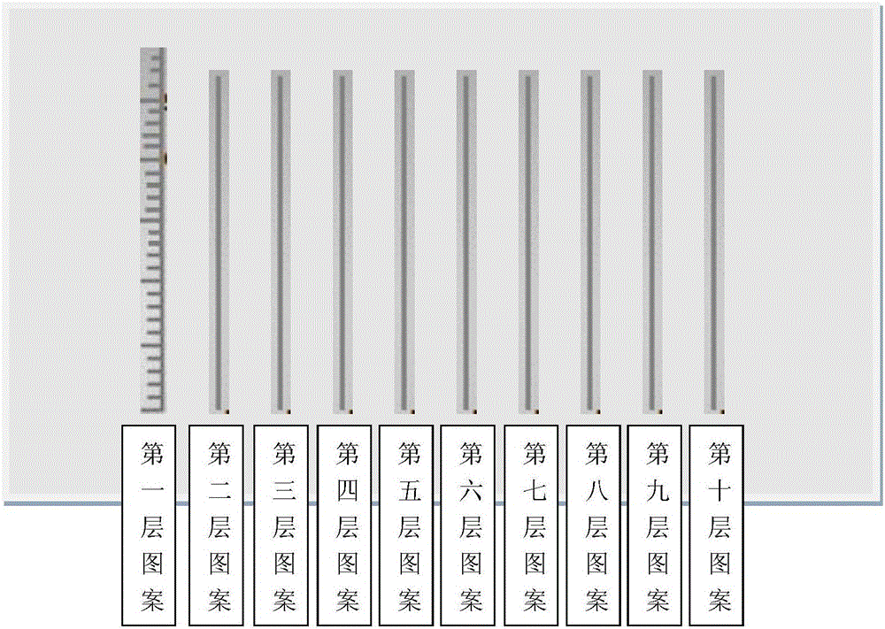
[0036] For example, in the manufacturing process of a liquid crystal display panel, 10 layers of film patterns need to be formed on the mother substrate. The first layer is a metal film layer, the second layer is a metal film layer, and the third to tenth layers are non-metal film layers. The film is a copper-titanium alloy film, which is yellow in color and dark in color, which is difficult to distinguish from the photoresist with the naked eye. The non-metallic film layer is composed of SiNx, SiO 2 Or IGZO material, the color is lighter and more transparent, and it can be easily distinguished from the photoresist with the naked eye.

[0037]For each scan (scanning), 10 masks are required to form 10 layers of thin film patterns, which are respectively named as the first mask, the second mask, ... the tenth mask, corresponding to the different layers formed Thin film patterns, that is, the first mask is used to form the first layer of thin film patterns, the second mask is use...

Embodiment 2

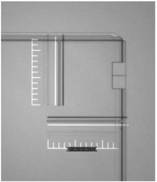
[0041] For example, an N-layer thin film pattern needs to be formed on the mother substrate during the manufacturing process of a liquid crystal display panel. The N-layer thin film consists of multiple metal film layers (copper-titanium alloy film, yellow) and multiple non-metallic film layers (translucent in color). or transparent) composition, peripheral exposure, such as Image 6 , The surrounding pattern of the first layer of film is a measuring scale, and a single row of patterns is conducive to clear reading of other layers. The positions of peripheral patterns from the second layer to the next metal film layer overlap and share a column of patterns. If the next layer of the metal film layer is still a metal film layer, the surrounding patterns of the next layer of the metal film layer are still separately formed into a row of patterns; The peripheral patterns of the next metal film layer overlap with each other, share a row of patterns, and so on. If the second layer...


PUM


Abstract

The invention discloses a periphery exposure method in manufacturing of a liquid crystal display panel. The method comprises the step of exposing the peripheral area of a mask plate, thereby forming N layers of film peripheral patterns on a main substrate, wherein N is more than or equal to 3; N layers of films are composed of dark color material film layers and light color material film layers; a measuring ruler is arranged on the peripheral pattern on the first layer of film; in the second to Nth layers, the upper and lower adjacent light color material film layers form a light color material film layer set; at least two layers of peripheral pattern positions in the light color material film layer set are locally or fully overlapped; the peripheral patterns of the dark color material film layers are not overlapped with the peripheral patterns of any light color material film layers above the dark color material film layers; the peripheral pattern positions of any two dark color material film layers are not overlapped. According to the periphery exposure method, the use area of each substrate with independent peripheral pattern is reduced and the use ratio of effective area of the main substrate is increased.

Description

technical field [0001] The invention belongs to the field of display technology, in particular to a peripheral exposure method in the manufacture of liquid crystal display panels. Background technique [0002] With the rapid development of the liquid crystal industry, panel sizes have become more diversified; followed by high investment in the early stage, which must be satisfied by high returns in the later stage. Therefore, how to maximize benefits is a topic that policy makers pay attention to first. To a large extent, improving substrate utilization is a priority for R&D departments. In addition, since each size has the problem of high space utilization and small remaining space, we should find ways to save the substrate area from other aspects. [0003] Usually, in the panel manufacturing process, it is necessary to form a multi-layer thin film pattern on the mother substrate, that is, it is necessary to use multiple masks to superimpose exposure processing one by one...

Claims


Application Information

Patent Timeline
Patent Type & Authority Applications(China)
IPC IPC(8): G03F7/20G02F1/1333
CPCG02F1/1333G03F7/70216
Inventor 王强
Owner NANJING CEC PANDA LCD TECH
Why Eureka
Try Eureka