AMOLED display panel and display device thereof
A technology for display panels and array substrates, applied in semiconductor devices, electrical components, circuits, etc., can solve problems affecting the image quality of display devices, achieve the effects of solving the Newton ring effect, reducing process costs, and improving image quality and yield
- Summary
- Abstract
- Description
- Claims
- Application Information
AI Technical Summary
Problems solved by technology
Method used
Image
Examples
Embodiment 1
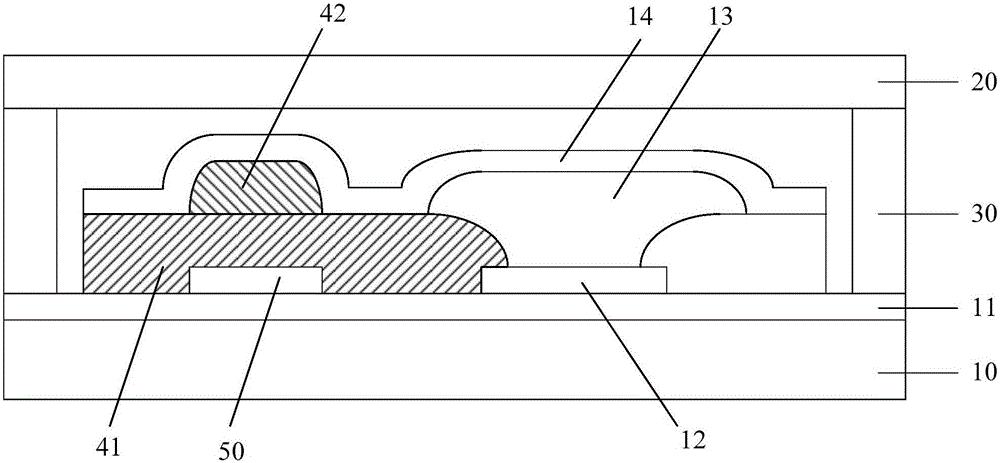
[0024] Please refer to figure 1 , which is a schematic structural diagram of the AMOLED display panel provided in Embodiment 1 of the present invention. like figure 1 As shown, the AMOLED display panel includes: an array substrate 10, a transparent substrate 20 opposite to the array substrate 10, a sealing material 30 connecting the array substrate 10 and the transparent substrate 20, the array substrate 10 and the transparent substrate A plurality of pillars are arranged between 20, and the pillars are used to resist pressure and maintain the thickness of the box. The pillars are formed by laminating at least two layers of pillars, wherein at least one layer of pillars is made of electrostrictive material, and the The top and bottom of the pillars are respectively provided with electrodes.
[0025] An electric field is formed between electrodes arranged on the top and bottom of the pillar, and the height of the sub-pillars made of electrostrictive material is controlled by ...
Embodiment 2
[0032] On the basis of the first embodiment, among the electrodes located on the upper and lower sides of the pillar, the electrode on the side close to the glass substrate is located on the glass substrate.
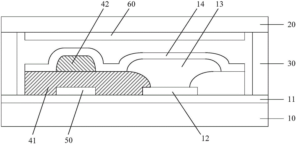
[0033] Please refer to figure 2, which is a schematic structural diagram of the AMOLED display panel provided in Embodiment 2 of the present invention. like figure 2 As shown, the AMOLED display panel includes: an array substrate 10, a transparent substrate 20 opposite to the array substrate 10, a sealing material 30 connecting the array substrate 10 and the transparent substrate 20, the array substrate 10 and the transparent substrate A plurality of pillars are arranged between 20, and the pillars are used to resist pressure and maintain the thickness of the box. The pillars are formed by laminating at least two layers of pillars, wherein at least one layer of pillars is made of electrostrictive material, and the The top and bottom of the pillars are respectively pr...
PUM
 Abstract
Description
Claims
Application Information

