Reaction cavity and semiconductor processing device

A reaction chamber and process chamber technology, which is applied in the manufacture of semiconductor/solid state devices, discharge tubes, electrical components, etc., can solve the problems of inductively coupled plasma ignition difficulty, unfavorable process stability, deterioration of etching uniformity, etc. Achieve the effect of avoiding high ignition voltage damage to the substrate, avoiding high ignition voltage and improving etching uniformity

Inactive Publication Date: 2017-01-04
BEIJING NAURA MICROELECTRONICS EQUIP CO LTD
View PDF4 Cites 12 Cited by
  • Summary
  • Abstract
  • Description
  • Claims
  • Application Information

AI Technical Summary

Problems solved by technology

[0005] In order to achieve uniform physical etching results, the above pre-cleaning process usually needs to be carried out at a lower process pressure (about 1mT), but the lower process pressure will make it difficult to start the inductively coupled plasma, or even fail to start at all. , therefore, the process needs to be divided into two steps of initiation and process, and this will have the following problems:
[0006] First, in the ignition step, the process pressure is high (above 10mT), the free paths of various particles are short, and the directionality of ions is poor. At this time, a negative bias voltage is applied to the carrier 10 to attract argon Ion bombardment

Method used


Image

  • Reaction cavity and semiconductor processing device
  • Reaction cavity and semiconductor processing device
  • Reaction cavity and semiconductor processing device

Examples


Example Embodiment

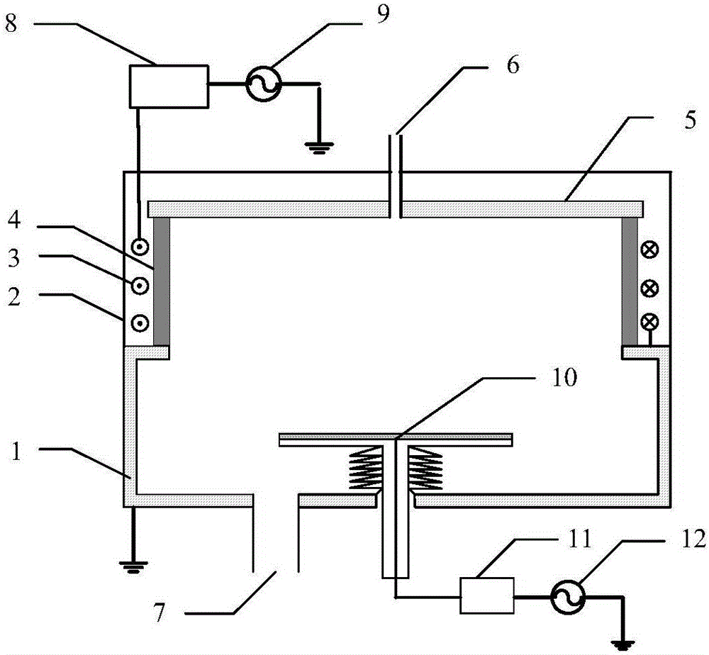
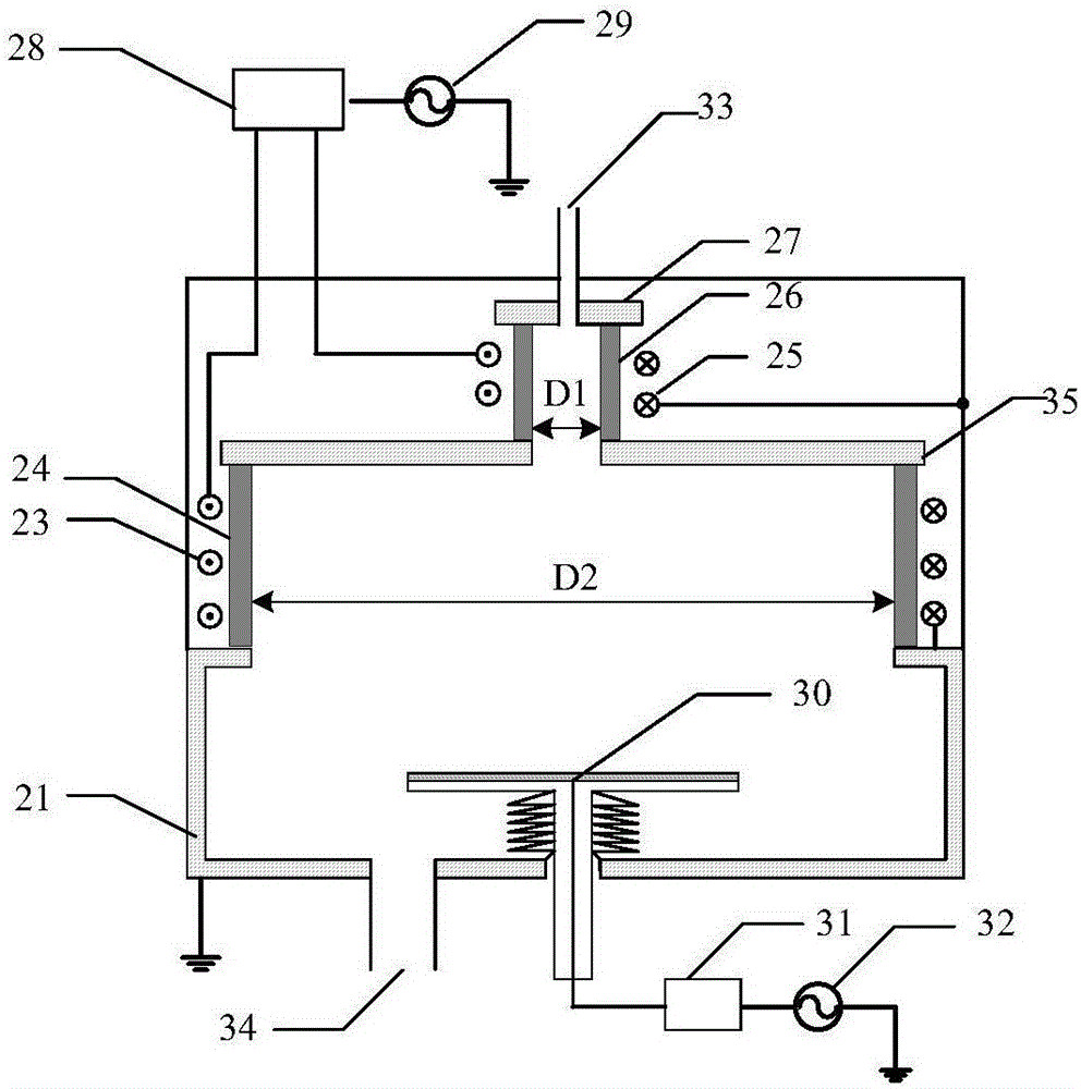
[0024] In order for those skilled in the art to better understand the technical solution of the present invention, the reaction chamber and semiconductor processing equipment provided by the present invention will be described in detail below in conjunction with the accompanying drawings.

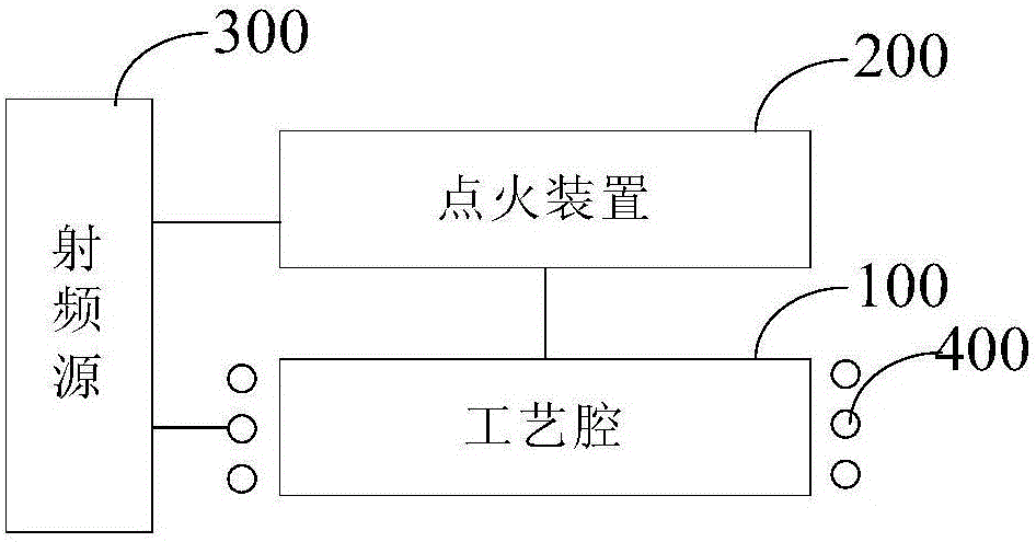
[0025] figure 2 Schematic block diagram of the reaction chamber provided for the present invention. see figure 2 , the reaction chamber includes a process chamber 100 for generating plasma, an ignition device 200 and a radio frequency source 300, wherein a first radio frequency coil 400 is arranged around the process chamber 100 . The ignition device 200 is disposed on the top of the process chamber 100 for igniting the plasma located in the part of the ignition device 200 . The radio frequency source 300 is used to respectively provide radio frequency energy to the first radio frequency coil 400 and the ignition device, and by distributing and adjusting the radio frequency energy obtai...


PUM

PropertyMeasurementUnit
The inside diameter ofaaaaaaaaaa

Abstract

The invention provides a reaction cavity and a semiconductor processing device. The reaction cavity comprises a technical cavity for generating plasmas, an ignition device arranged at the top of the technical cavity and an RF source; the ignition device starts the plasmas positioned in part of the ignition device; and the RF source provides an RF energy to a first RF coil and the ignition device, adjusts distribution of the RF energy obtained by the first RF coil and the ignition device, and starts the plasmas in part of the ignition device and in the technical cavity sequentially. The reaction cavity provided by the invention ensure smooth starting, keeps the technical air pressure in the technical cavity constant, and thus, improves the total technical stability. In the starting process, the technical air pressure in the technical cavity is relatively low, the etching uniformity can be improved, and a substrate is prevented from damage caused by relatively high starting voltage.

Description

technical field [0001] The invention relates to the field of semiconductor manufacturing, in particular to a reaction chamber and semiconductor processing equipment. Background technique [0002] In the semiconductor manufacturing process, the inductively coupled plasma (ICP) equipment can obtain high-density plasma at a low working pressure, and has a simple structure and low cost. (determines the plasma density) and the substrate stage radio frequency source (determines the particle energy incident on the wafer) is independently controlled, therefore, ICP equipment is widely used in plasma etching (IC), physical vapor deposition (PVD), plasma Chemical Vapor Deposition (CVD), Micro Electro Mechanical Systems (MEMS) and Light Emitting Diodes (LED) and other processes. [0003] Currently, in the pre-cleaning process, inductively coupled plasma is usually used to generate high-density plasma to process the substrate. The composition of the pre-cleaning chamber is as follows ...

Claims


Application Information

Patent Timeline
IPC IPC(8): H01J37/32H01L21/67
Inventor 张彦召陈鹏
Owner BEIJING NAURA MICROELECTRONICS EQUIP CO LTD
Why Eureka
Try Eureka