Semiconductor integrated circuit spiral inductor

A technology of integrated circuits and spiral inductors, applied in semiconductor devices, circuits, semiconductor/solid-state device components, etc., can solve the problems of poor quality factor of spiral inductors, and achieve the effect of improving quality factor, reducing loss, and integrating process compatibility.

Active Publication Date: 2018-11-20
NO 24 RES INST OF CETC
View PDF8 Cites 0 Cited by
  • Summary
  • Abstract
  • Description
  • Claims
  • Application Information

AI Technical Summary

Problems solved by technology

[0003] The invention provides a semiconductor integrated circuit spiral inductor to solve the problem of poor quality factor of the current semiconductor integrated circuit spiral inductor

Method used


Image

  • Semiconductor integrated circuit spiral inductor
  • Semiconductor integrated circuit spiral inductor
  • Semiconductor integrated circuit spiral inductor

Examples


Embodiment Construction

[0025] In order to enable those skilled in the art to better understand the technical solutions in the embodiments of the present invention, and to make the above-mentioned purposes, features and advantages of the embodiments of the present invention more obvious and understandable, the following describes the technical solutions in the embodiments of the present invention in conjunction with the accompanying drawings For further detailed explanation.

[0026] In the description of the present invention, unless otherwise specified and limited, it should be noted that the term "connection" should be understood in a broad sense, for example, it can be a mechanical connection or an electrical connection, or it can be the internal communication of two elements, it can be Directly connected or indirectly connected through an intermediary, those skilled in the art can understand the specific meanings of the above terms according to specific situations.

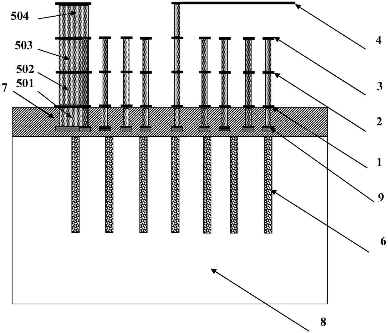
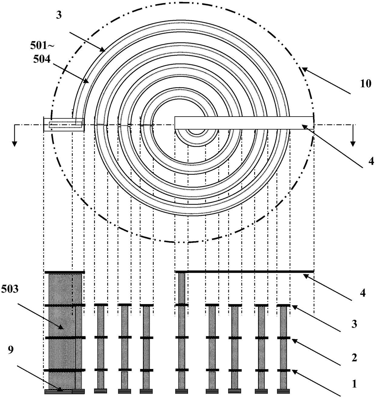
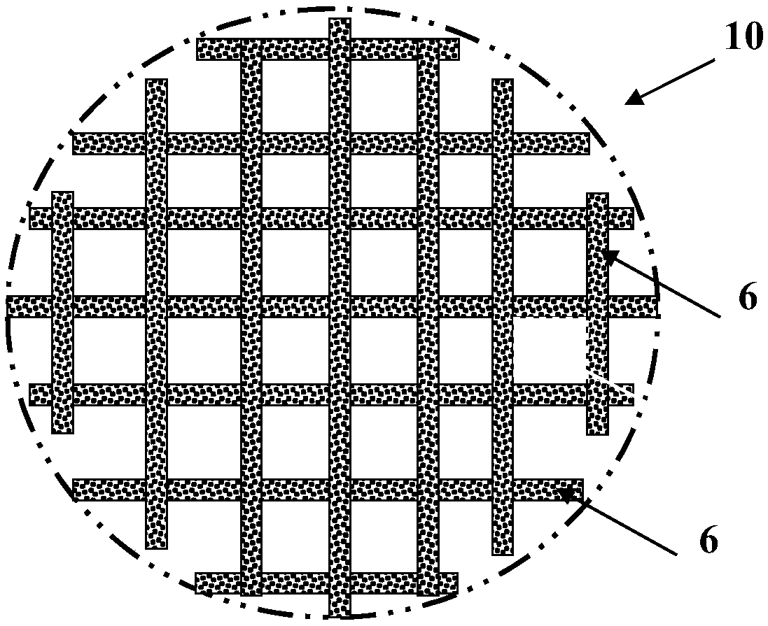
[0027] In the embodiment of ...


PUM


Abstract

The invention provides a spiral inductor of a semiconductor integrated circuit. The spiral inductor comprises a substrate, a plurality of layers of dielectric layers, and metal wiring layers, the plurality of layers of dielectric layers are formed on the substrate, the metal wiring layer is formed on each dielectric layer, each dielectric layer is provided with a spiral through groove, the through groove is filled with tungsten metal to form a tungsten metal wall in each dielectric layer, the tungsten metal walls in the dielectric layers are mutually overlapped, and the metal wiring layers are used for connecting the tungsten metal walls in the dielectric layers. According to the spiral inductor, the plurality of layers of dielectric layers with the spiral tungsten metal walls are designed, the tungsten metal walls in the dielectric layers are mutually connected through the metal wiring layers between the dielectric layers, the thickness of spiral inductor coils can be increased, the coil metal resistance loss of the spiral inductor and the loss caused by the skin effect can be reduced, and the quality factor of the spiral inductor can be increased.

Description

technical field [0001] The invention belongs to the field of semiconductor integrated circuits, in particular to a semiconductor integrated circuit spiral inductor. Background technique [0002] In the existing semiconductor integrated circuit multilayer metal wiring process, such as SiGe BiCMOS, BiCMOS or CMOS process, because of the requirements of radio frequency design and high integration, it is often necessary to be compatible with integrated on-chip passive inductance. In order to improve the performance of this on-chip passive inductance, Such inductors are required to have lower losses and higher inductance quality factors. However, the quality factor of passive inductors in existing common semiconductor integrated circuits is relatively low. Contents of the invention [0003] The invention provides a semiconductor integrated circuit spiral inductor to solve the problem of poor quality factor of the current semiconductor integrated circuit spiral inductor. [00...

Claims


Application Information

Patent Timeline
Patent Type & Authority Patents(China)
IPC IPC(8): H01L23/522
Inventor 谭开洲崔伟杨永晖朱坤峰张霞黄东钱呈梁柳洪汪璐张静陈俊韩卫敏吴雪刘娇
Owner NO 24 RES INST OF CETC
Why Eureka
Try Eureka