Memory component and manufacturing method thereof

A technology for memory elements and manufacturing methods, applied in semiconductor/solid-state device manufacturing, electrical components, electric solid-state devices, etc., capable of solving problems such as high contact resistance and limited process margin

Active Publication Date: 2017-01-04
MACRONIX INT CO LTD
View PDF4 Cites 5 Cited by
  • Summary
  • Abstract
  • Description
  • Claims
  • Application Information

AI Technical Summary

Problems solved by technology

[0004] However, in order to provide better device control performance, the thickness of the channel layer 104 is generally relatively thin, so that the process window is quite limited (even insufficient) when defining the metal contact structure 106 on the channel layer 104.
In addition, the channel layer 104 is generally made of polysilicon, which will form a metal silicide (silicide) junction with the barrier layer of the metal contact structure 106. Too thin channel layer 104 will easily cause voids (voids) at the metal silicide junction. ), resulting in the problem of high contact resistance between the metal contact structure 106 and the channel layer 104

Method used


Image

  • Memory component and manufacturing method thereof
  • Memory component and manufacturing method thereof
  • Memory component and manufacturing method thereof

Examples


Embodiment Construction

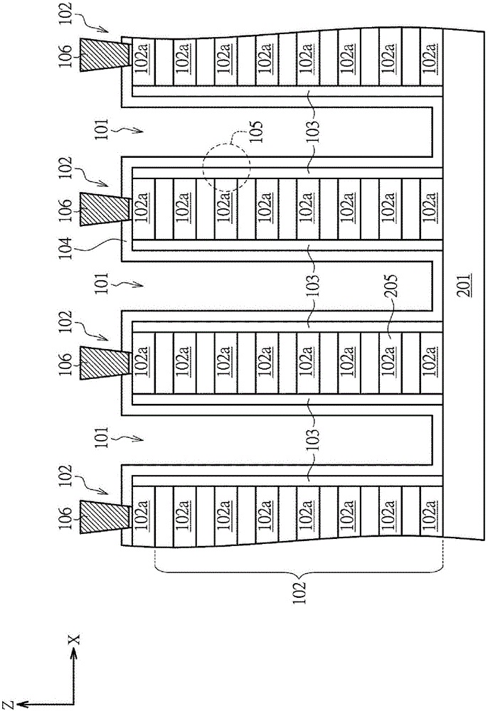
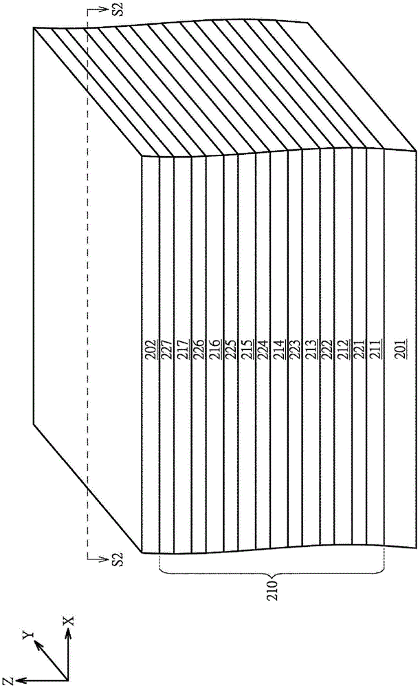
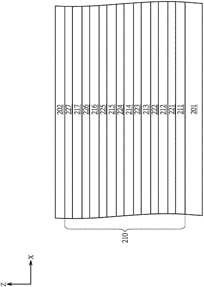
[0033] The invention provides a three-dimensional memory element and its manufacturing method, which can provide a large process margin for the three-dimensional memory element to form a metal contact structure, and at the same time reduce the contact resistance of the metal contact structure. In order to make the above-mentioned embodiments and other objects, features and advantages of the present invention more comprehensible, the digital 3D memory device and its manufacturing method are specifically cited below as preferred embodiments and described in detail with the accompanying drawings.

[0034] However, it must be noted that these specific implementation cases and methods are not intended to limit the present invention. The invention can still be implemented with other features, elements, methods and parameters. The proposal of the preferred embodiment is only used to illustrate the technical characteristics of the present invention, and is not used to limit the patent...


PUM


Abstract

The invention discloses a memory component and a manufacturing method thereof. The memory component comprises a patterned multilayer stack structure, a semiconductor coverage layer, a storage material layer and a channel layer; the patterned multilayer stack structure is positioned on a substrate, includes at least one channel to define ridge-shaped multi-lamination layers, and each ridge-shaped multi-lamination layer comprises a conducting strip at least; the semiconductor coverage layer covers the ridge-shaped multi-lamination layers; the storage material layer covers the sidewall of a channel; and the channel layer covers the storage material layer, the semiconductor coverage layer and the bottom of the channel, and makes direct contact with the semiconductor coverage layer.

Description

technical field [0001] The present invention relates to a non-volatile memory (non-volatile memory) element and a manufacturing method thereof, in particular to a three-dimensional (Three-Dimension, 3D) non-volatile memory element and a manufacturing method thereof. Background technique [0002] A non-volatile memory (Non-Volatile Memory, NVM) element, such as a flash memory, has the characteristic that the information stored in the memory unit will not be lost when the power is removed. It has been widely used in solid-state mass storage applications for portable music players, mobile phones, digital cameras, etc. Three-dimensional non-volatile memory elements, such as vertical-channel (Vertical-Channel, VC) three-dimensional NAND flash memory elements, have many layer stack structures, which can achieve higher storage capacity and have excellent electronic characteristics, such as good data Preserve reliability and speed of operation. [0003] A typical three-dimensional...

Claims


Application Information

Patent Timeline
Patent Type & Authority Applications(China)
IPC IPC(8): H01L27/115H01L21/8247
Inventor 李冠儒
Owner MACRONIX INT CO LTD
Why Eureka
Try Eureka