Schottky contact and preparation method thereof
A technology of Schottky contact and ohmic contact, which is applied in the manufacture of semiconductor/solid-state devices, electrical components, circuits, etc., can solve the problems of not being able to obtain good results, and the MIS sandwich structure does not have good heat resistance, so as to avoid costs Rice level pinning effect, effect of good device characteristics
- Summary
- Abstract
- Description
- Claims
- Application Information
AI Technical Summary
Problems solved by technology
Method used
Image


Examples
Embodiment Construction
[0033] The specific implementation manners of the present invention will be further described in detail below in conjunction with the accompanying drawings and embodiments. The following examples are used to illustrate the present invention, but are not intended to limit the scope of the present invention.
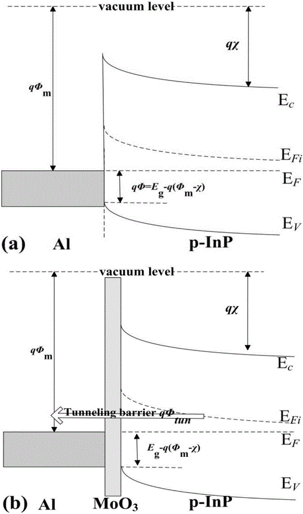
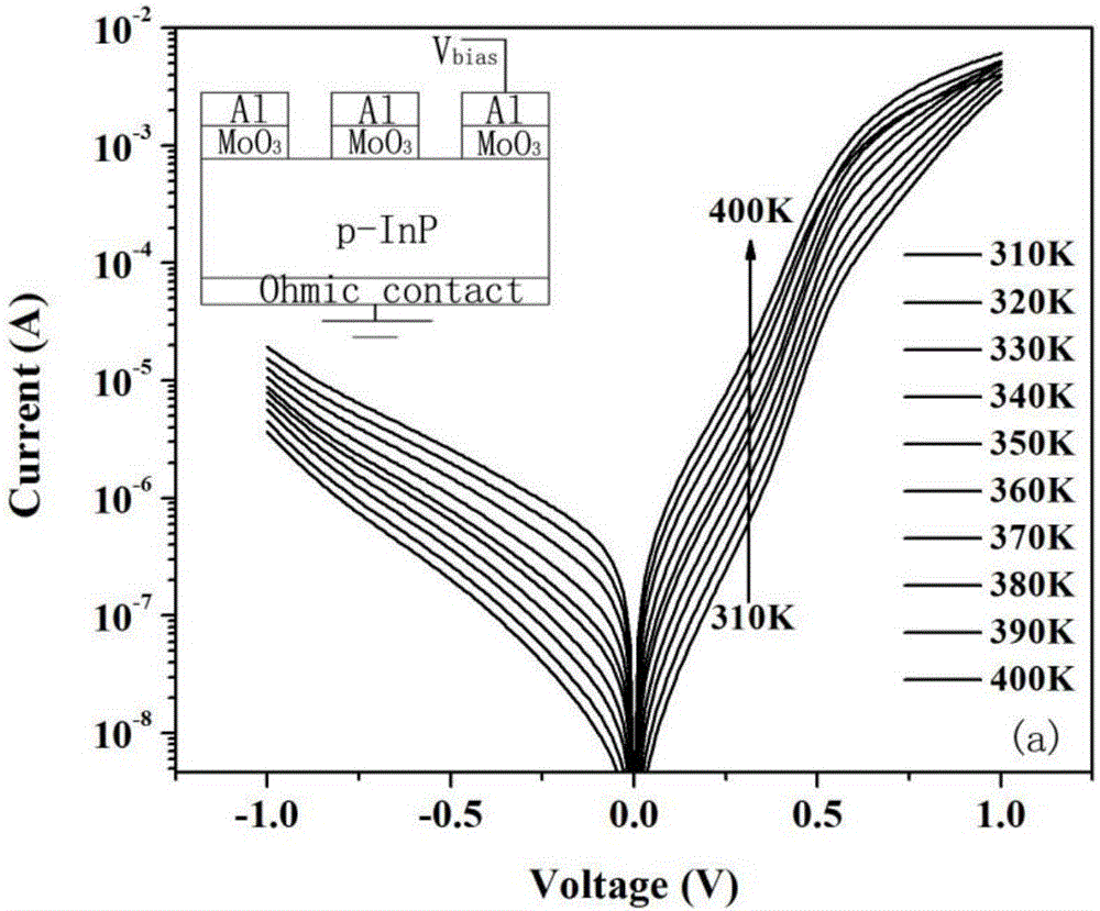
[0034] A Schottky contact of the present invention includes a p-InP substrate, an insulating dielectric layer and an electrode metal layer, an ohmic contact metal layer is grown on the p-InP substrate, and the insulating dielectric layer is MoO 3 . With MoO 3 The thickness of the insulating medium layer is 3-4nm; the ohmic contact metal layer is a compound metal layer of Ti, Pt and Au; the electrode metal layer is metal Al.
[0035] The present invention selects MoO 3 Prepared Al / MoO with MIS structure as insulating dielectric layer 3 / p-InP Schottky contact, for testing MoO 3 The influence of the insulating dielectric layer on the metal / p-InP Schottky contact, and th...
PUM
| Property | Measurement | Unit |
|---|---|---|
| Thickness | aaaaa | aaaaa |
Abstract
Description
Claims
Application Information