A self-driven photodetector with low dark current and its preparation method
A photodetector, dark current technology, applied in circuits, electrical components, semiconductor devices, etc., can solve the problems of difficult to achieve infrared band detection, large forbidden band width, etc., to avoid Fermi level pinning effect, good light Responsive, effect of good photovoltaic properties
- Summary
- Abstract
- Description
- Claims
- Application Information
AI Technical Summary
Problems solved by technology
Method used
Image

Examples
Embodiment 1
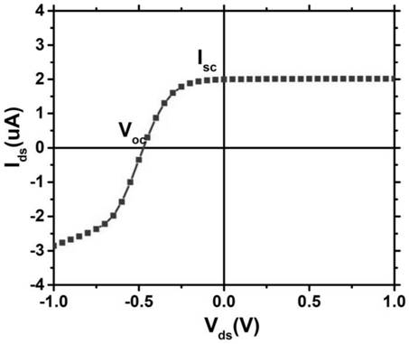
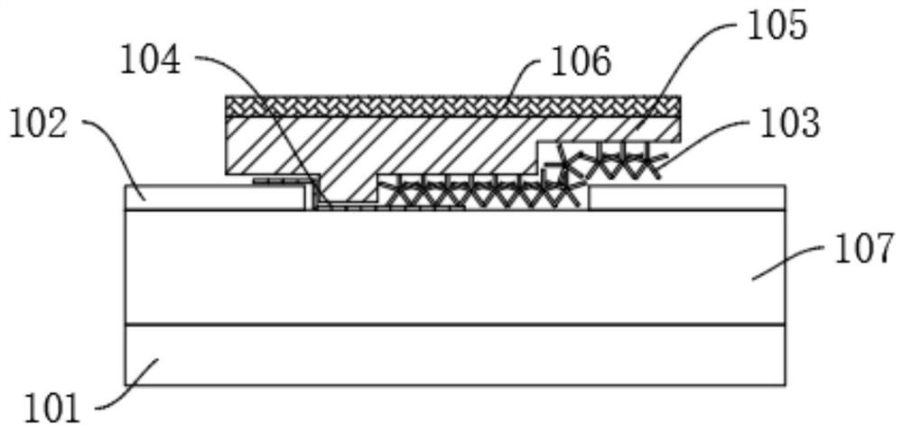
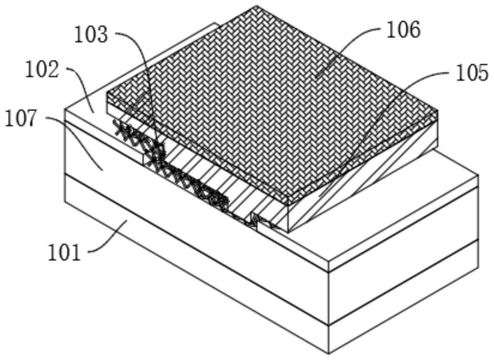
[0035] refer to Figure 1-3 , the present invention provides a self-driven photodetector with low dark current, including a substrate 101 and a two-dimensional semiconductor material sheet transferred on the substrate, two metal electrodes 102, a tunneling layer 105 and a trapping layer 106 , the two metal electrodes 102 are respectively deposited on both sides of the substrate, the tunneling layer 105 is located at the top of the heterojunction of the two-dimensional semiconductor material, and the trapping layer 106 is located above the tunneling layer 105; the two-dimensional semiconductor The material flakes are transition metal chalcogenides WSe 2 103 and graphene 104, the material of the tunneling layer 105 is HfO 2 , the trapping layer 106 material is Si 3 N 4 .
[0036] Transition metal chalcogenide WSe in two-dimensional semiconductor material flakes in the present invention 2 The thickness of 103 and graphene 104 is 50nm, and the deviation is not more than 1%....
PUM
 Abstract
Description
Claims
Application Information