
Preparation method of cobalt-doped amorphous carbon film/silicon photovoltaic device

An amorphous carbon film and device technology, applied in the field of cobalt-doped amorphous carbon film/silicon photovoltaic device and its preparation, can solve the problems of poor corrosion resistance and reuse performance, high production cost, long production cycle, etc. Low cost, high working stability and low cost

Active Publication Date: 2016-06-01
HUAIYIN TEACHERS COLLEGE
View PDF4 Cites 0 Cited by
  • Summary
  • Abstract
  • Description
  • Claims
  • Application Information

AI Technical Summary

Problems solved by technology

They also have defects such as high production cost, long production cycle, fragile outdoor use, poor corrosion resistance and poor reusability.

Method used


Image

  • Preparation method of cobalt-doped amorphous carbon film/silicon photovoltaic device
  • Preparation method of cobalt-doped amorphous carbon film/silicon photovoltaic device
  • Preparation method of cobalt-doped amorphous carbon film/silicon photovoltaic device

Examples


Embodiment Construction

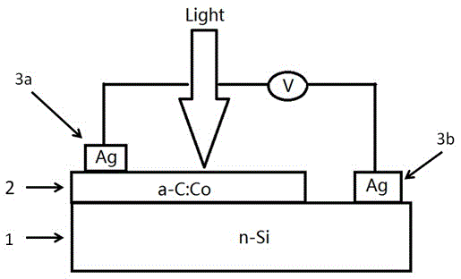
[0019] Prototypes are made according to the above-mentioned technical scheme. The N-type silicon (n-Si) substrate is a phosphorus-doped n-Si substrate, and its resistivity is 8-13Ω·cm. On one area of ​​the substrate (the upper surface of one end of the substrate), a cobalt-doped amorphous carbon a-C:Co film was prepared by pulsed laser deposition using 99.99% pure graphite and 99.9% metallic Co as targets. Source, the metal Co sheet is pasted on the graphite target. During operation, uniform doping is achieved by the rotation of the target and the sample substrate. The Co doping amount is about 10%, the laser energy is 320 mJ / pulse, and the vacuum degree of the cavity is 1×10 -4 mBar, the substrate temperature is 400°C, the distance between the target and the substrate is 5cm, the temperature is naturally cooled to room temperature after coating, and the film thickness is about 25nm. Then adopt the vacuum thermal evaporation method, by the control of the mask plate, on the pr...


PUM

PropertyMeasurementUnit
electrical resistivityaaaaaaaaaa
thicknessaaaaaaaaaa
thicknessaaaaaaaaaa

Abstract

The invention provides a cobalt-doped non-crystalline carbon film / silicon photovoltaic device and a manufacturing method thereof. The method comprises the steps that an n-Si substrate is used as a substrate, and two areas are preformed in the upper surface of the substrate; in one area, the cobalt-doped non-crystalline carbon (a-C:Co) film is manufactured with a pulsed laser deposition method, then an Ag layer is evaporated on the carbon film with a vacuum thermal evaporation method; in the other area, the Ag layer is directly evaporated on the n-Si substrate with the vacuum thermal evaporation method, and the silicon photovoltaic device is manufactured. Through the test, the device shows good photovoltaic characteristics and shows the best photovoltaic characteristics at room temperature, the temperature has little influence on the photovoltaic effect when greater than 270 K(-3 DEG C), and the device has the advantages of being slightly affected by the environment temperature and high in work stability. The device is easy to recycle and reuse; the non-crystalline carbon film is good in corrosion resistance and abrasion resistance, can be combined with surface materials of a building, and greatly saves installation space; in addition, adopted materials are low in price, the manufacturing technology is simple, no pollutant is produced, and environment protection is facilitated.

Description

technical field [0001] The invention relates to photovoltaic technology, in particular to a cobalt-doped amorphous carbon film / silicon photovoltaic device and a preparation method thereof. technical background [0002] Photovoltaic device is an electronic device that converts sunlight energy into electrical energy based on the principle of photovoltaic effect, and is the core part of solar cells. It is generally composed of two semiconductor materials to form a P-N junction. When sunlight shines on the device, a potential difference is generated at both ends of the P-N junction, which can supply power to an external load and convert solar energy into electrical energy. In view of the fact that solar energy is an inexhaustible clean energy, the electricity obtained through photovoltaic devices has the advantage of no pollution to the environment, so photovoltaic devices are widely used in various fields such as national defense, scientific research, industrial and agricultura...

Claims


Application Information

Patent Timeline
Patent Type & Authority Patents(China)
IPC IPC(8): H01L31/0216H01L31/0224H01L31/04H01L31/20
CPCH01L31/0288H01L31/202Y02B10/10Y02E10/50Y02P70/50
Inventor 翟章印江成姜昱丞陈贵宾
Owner HUAIYIN TEACHERS COLLEGE
Learn More