
Self-driven photoelectric detector with low dark current and preparation method thereof

A photodetector, dark current technology, applied in circuits, electrical components, semiconductor devices, etc., can solve the problems of large forbidden band width, difficult to achieve infrared band detection, etc., achieve good photoresponse, and avoid Fermi level pinning effect, the effect of good photovoltaic properties

Active Publication Date: 2020-08-07
SOUTH CHINA UNIV OF TECH
View PDF5 Cites 0 Cited by
  • Summary
  • Abstract
  • Description
  • Claims
  • Application Information

AI Technical Summary

Problems solved by technology

However, due to the relatively large band gap of silicon semiconductors, it is difficult to detect in the infrared band.

Method used


Image

  • Self-driven photoelectric detector with low dark current and preparation method thereof
  • Self-driven photoelectric detector with low dark current and preparation method thereof
  • Self-driven photoelectric detector with low dark current and preparation method thereof

Examples


Embodiment 1

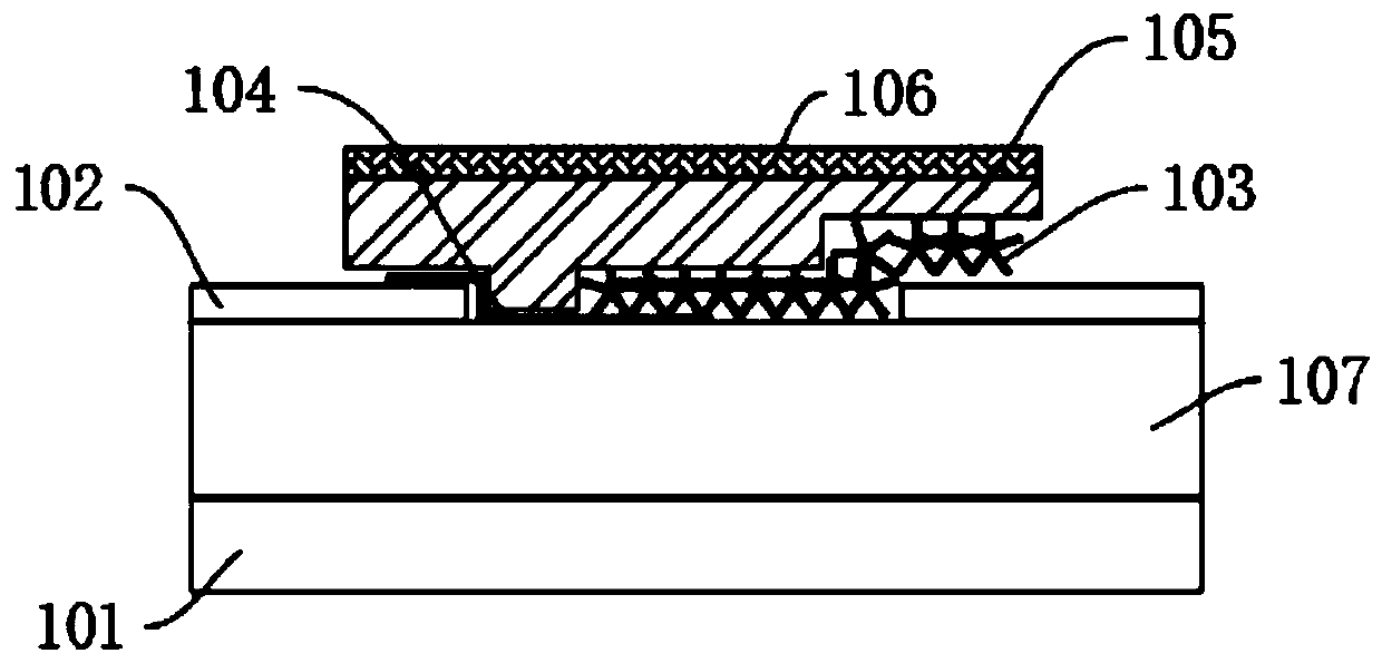
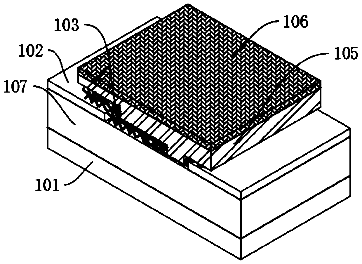
[0035] refer to Figure 1-3 , the present invention provides a self-driven photodetector with low dark current, including a substrate 101 and a two-dimensional semiconductor material sheet transferred on the substrate, two metal electrodes 102, a tunneling layer 105 and a trapping layer 106 , the two metal electrodes 102 are respectively deposited on both sides of the substrate, the tunneling layer 105 is located at the top of the heterojunction of the two-dimensional semiconductor material, and the trapping layer 106 is located above the tunneling layer 105; the two-dimensional semiconductor The material flakes are transition metal chalcogenides WSe 2 103 and graphene 104, the material of the tunneling layer 105 is HfO 2 , the trapping layer 106 material is Si 3 N 4 .

[0036] Transition metal chalcogenide WSe in two-dimensional semiconductor material flakes in the present invention 2 The thickness of 103 and graphene 104 is 50nm, and the deviation is not more than 1%....


PUM


Abstract

The invention discloses a self-driven photoelectric detector with low dark current and a preparation method thereof, and belongs to the field of semiconductor devices and manufacturing thereof. A Graphene-WSe2-Au structure device prepared by a deterministic dry transfer method has good photovoltaic characteristics, the Fermi level pinning effect easily caused by the direct evaporation of an electrode on a two-dimensional material in a traditional method is avoided, and the device has good photoresponse. The two heterojunction WSe2-Graphene junctions and the WSe2-Au junction of the device haveasymmetry, so that the device has a self-driving characteristic and can work under zero bias voltage, and at the moment, dark current can be almost ignored; moreover, due to the introduction of a tunneling layer and a trapping layer, the dark current can be controlled at a very low order of magnitude even if the device works under external bias.

Description

technical field [0001] The invention relates to the field of semiconductor devices and their manufacture, in particular to a self-driven photodetector with low dark current and a preparation method thereof. Background technique [0002] A photodetector is a detection device that converts an optical signal into an electrical signal, and has a very wide and important application in both military and civilian fields. In the military, it is mainly used in guidance, radar monitoring, optical communication, etc.; in civilian use, it also has important applications in camera, infrared detection, temperature measurement, etc. [0003] Currently, silicon-based photodetectors are the workhorse behind commercial image sensors embedded in mobile phones, computers, and digital cameras, especially PN junction-based photodiodes due to their manufacturing process compatibility with mainstream complementary metal-oxide-semiconductor (CMOS) technology. Increasingly common in consumer electro...

Claims


Application Information

Patent Timeline
Patent Type & Authority Applications(China)
IPC IPC(8): H01L31/11H01L31/032H01L31/0336H01L31/18
CPCH01L31/032H01L31/0336H01L31/11H01L31/18Y02P70/50
Inventor 周长见张首勇吕喆
Owner SOUTH CHINA UNIV OF TECH
Learn More