Semiconductor avalanche photoelectric detector using a low dimensional quantum dot multiplication layer

An avalanche optoelectronic and quantum dot layer technology, which is applied in the direction of semiconductor devices, circuits, electrical components, etc., can solve the problems of low device reliability, complicated preparation process, and large dark current, and achieve improved avalanche gain, less kinetic energy loss, and acoustic The effect of sub-scattering suppression

Inactive Publication Date: 2017-01-04
弦海(上海)量子科技有限公司
View PDF6 Cites 6 Cited by
  • Summary
  • Abstract
  • Description
  • Claims
  • Application Information

AI Technical Summary

Problems solved by technology

However, there are also certain problems, such as complex material p

Method used


Image

  • Semiconductor avalanche photoelectric detector using a low dimensional quantum dot multiplication layer
  • Semiconductor avalanche photoelectric detector using a low dimensional quantum dot multiplication layer
  • Semiconductor avalanche photoelectric detector using a low dimensional quantum dot multiplication layer

Examples


Embodiment 1

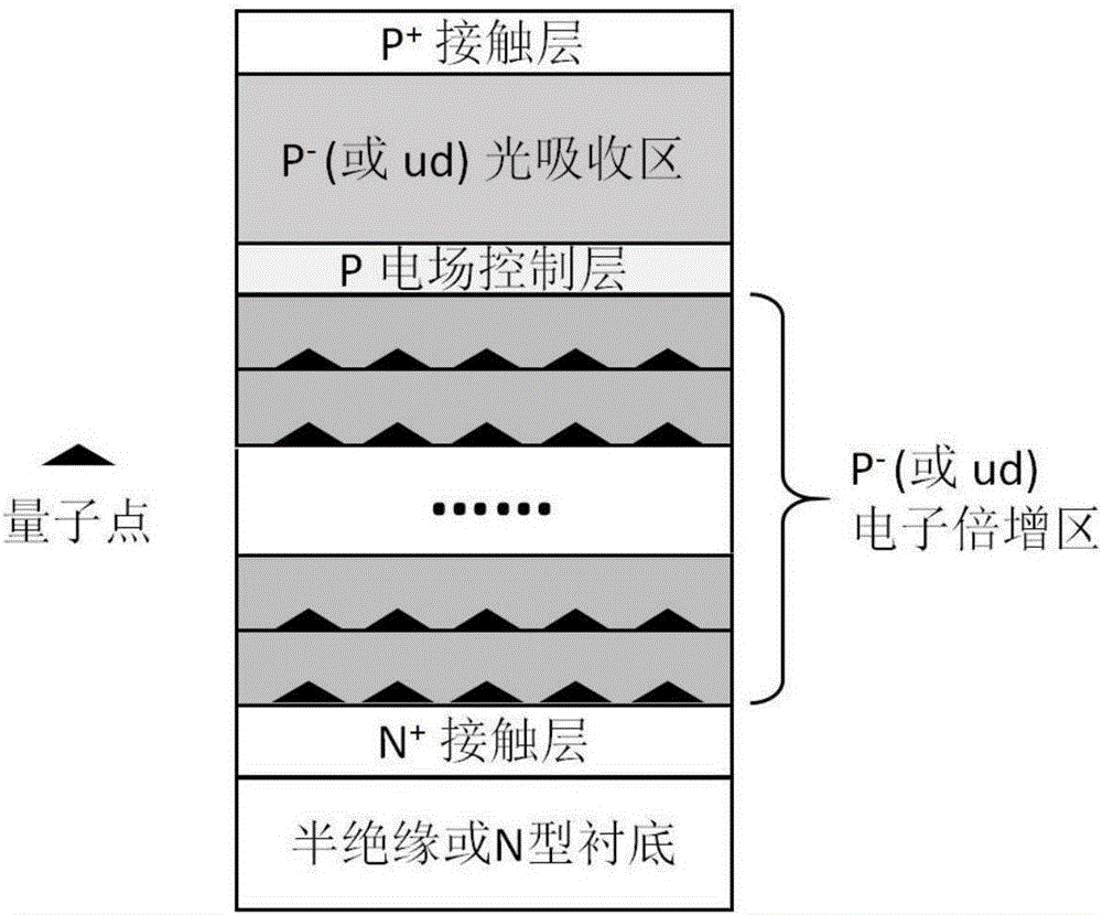
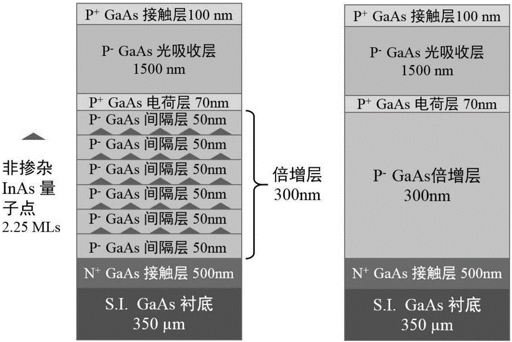
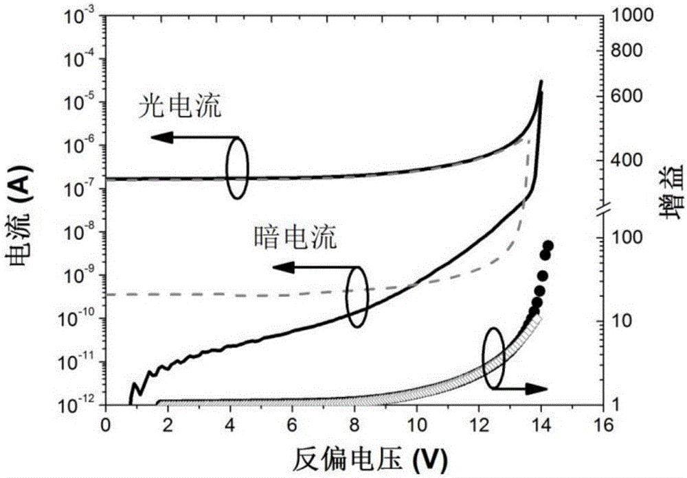
[0038] The purpose of this embodiment is to use InAs quantum dots as multiplier materials to improve the gain coefficient of GaAs APD and reduce its excess noise. The device is a mesa junction structure, adopts the basic structure of absorption multiplication and separation, uses electrons as multiplied carriers, and uses P + -P - -P +- P - -N + The doped structure of the device material is grown using a molecular beam epitaxy system. The feasibility of the present invention is verified by comparing with a control device without quantum dot multiplication. The specific device structures of quantum dot multiplication and non-quantum dot multiplication APD are as follows: figure 2 Shown left and right. Both device structure parameters are identical except for the multiplication region. Its structure contains the following materials in order from bottom to top:

[0039] ① Semi-insulating (S.I.) GaAs (001) substrate. The thickness is 350 microns, and the resistivity ρ≥1M...


PUM


Abstract

The invention relates to a semiconductor avalanche photoelectric detector using a low dimensional quantum dot multiplication layer. In the multiplication layer of the semiconductor avalanche photoelectric detector, there are several quantum dot layers which have a narrower band gap than the multiplication layer and form an I-type band structure with the multiplication layer materials. With the detector provided by the invention, the gain coefficient increases obviously; excess noise can be suppressed; and it can be widely used to enhance the performance of the avalanche detector in different bands such as Si-Ge, GaAs-InAs, InP-InGaAs, InAlAs-InGaAs, and GaAs-AlSb, and raise the application level of avalanche detector systems including high speed optical communication, single photon counting, laser radar, quantum information and etc.

Description

technical field [0001] The invention belongs to the field of semiconductor avalanche photodetectors, in particular to a semiconductor avalanche photodetector using a low-dimensional quantum dot multiplication layer. Background technique [0002] Semiconductor avalanche photodiode (Avalanche Photodiode, APD) is a high-sensitivity photodetector that utilizes carrier impact ionization multiplication effect to achieve internal photocurrent amplification. Its basic structure is a semiconductor photodiode working under a large reverse bias voltage, and the photocurrent gain in the device is realized by utilizing the collision ionization multiplication effect of photogenerated carriers in the depletion region. It can provide a photocurrent gain 5dB or more higher than that of the PIN detector. APD also has lower junction capacitance, so it can meet both high-speed response and high detection sensitivity. Depending on the semiconductor material used, APDs can cover different photo...

Claims


Application Information

Patent Timeline
IPC IPC(8): H01L31/107H01L31/0352
CPCH01L31/0352H01L31/035218H01L31/107
Inventor 马英杰张永刚顾溢陈星佑
Owner 弦海(上海)量子科技有限公司
Why Eureka
Try Eureka