Resistive random access memory and preparation method thereof

A resistive variable memory and resistive variable technology, applied in semiconductor/solid-state device manufacturing, semiconductor devices, electric solid-state devices, etc., can solve the problems of reducing the stability and reliability of resistive variable memory, increase the probability of conductive channels, improve Uniformity and the effect of improving stability

Active Publication Date: 2017-01-04
SUZHOU INST OF NANO TECH & NANO BIONICS CHINESE ACEDEMY OF SCI
View PDF3 Cites 7 Cited by
  • Summary
  • Abstract
  • Description
  • Claims
  • Application Information

AI Technical Summary

Problems solved by technology

Since this kind of fracture and formation is random, the morphology and distribution of conductive filaments are different during multiple resistance switching processes, so the electrical parameters of th

Method used


Image

  • Resistive random access memory and preparation method thereof
  • Resistive random access memory and preparation method thereof
  • Resistive random access memory and preparation method thereof

Examples


Embodiment 1

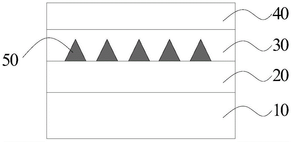
[0028] figure 1 is a schematic structural diagram of a resistive variable memory according to Embodiment 1 of the present invention.

[0029] refer to figure 1 , The resistive variable memory according to Embodiment 1 of the present invention includes a substrate 10; a first electrode 20, a resistive material layer 30, and a second electrode 40 sequentially stacked on the substrate 10; and, arranged on the first electrode The conductive protrusion array 50 formed on the surface of the first electrode 20 is spaced between the resistive material layer 30 and the resistive material layer 20 .

[0030] In this embodiment, the material of the above-mentioned conductive bump array 50 is Pt, and the height of the conductive bump array is about 5nm, and the pitch is 50nm; but the present invention is not limited thereto, the material of the conductive bump array can also be selected Any one of Cu, Al, Ti, Ni, Au, and the height of the conductive bump array is limited to 1nm-5nm, and...

Embodiment 2

[0050] In the description of Embodiment 2, the similarities with Embodiment 1 will not be repeated here, and only the differences with Embodiment 1 will be described. The difference between embodiment 2 and embodiment 1 is that, referring to Figure 5 , the resistive variable memory according to Embodiment 2 of the present invention includes a substrate 10; a first electrode 20, a resistive material layer 30, and a second electrode 40 sequentially stacked on the substrate 10; and, arranged on the second electrode 40 and the resistance-switching material layer 30 and spaced apart from the conductive bump array 50 formed on the surface of the resistance-switching material layer 30 .

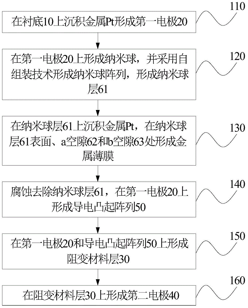
[0051] refer to Figure 6 A flow chart of the steps of the method for manufacturing the resistive variable memory according to Embodiment 2 of the present invention.

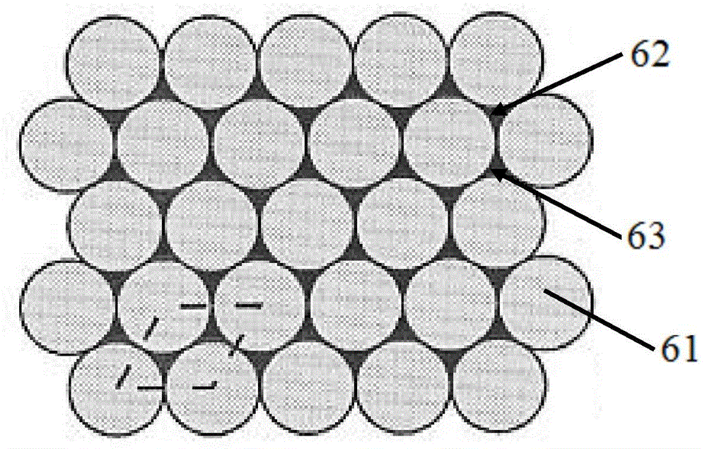
[0052] In step 210 , metal Pt is deposited on the substrate 10 to form the first electrode 20 , and the resistive material layer ...


PUM

PropertyMeasurementUnit
Heightaaaaaaaaaa
Spacingaaaaaaaaaa
Thicknessaaaaaaaaaa

Abstract

The present invention discloses a resistive random access memory. The resistive random access memory comprises a first electrode, a resistive random material layer and a second electrode arranged on a substrate in order, and also comprises a conductive bumping array formed at the interface of the first electrode and the resistive random material layer or/and the interface of the second electrode and the resistive random material layer at intervals. The resistive random access memory prepares a uniformly distributed and controllable conductive bumping array at the interface of the first electrode or/and the second electrode and the resistive random material layer to allow an electric field to integrate on the conductive bumping array and increase the probability of forming a conductive channel at the conductive bumping array so as to improve the work stability of the resistive random access memory and improve the uniformity of the resistive random access memory. The present invention further discloses the preparation method of the resistive random access memory, and comprises: A, the step of preparing the first electrode, the resistive random material layer and the second electrode on the substrate; and B, the step of preparing the conductive bumping array at the interface of the first electrode and the resistive random material layer or/and the second electrode and the resistive random material layer.

Description

technical field [0001] The invention belongs to the technical field of integrated circuits, and in particular relates to a resistive variable memory capable of improving the uniformity of the resistive variable memory and a preparation method thereof. Background technique [0002] Resistive RAM (RRAM) has the advantages of simple structure, fast read and write speed, low operating power consumption, high storage density, compatibility with existing CMOS (complementary metal oxide semiconductor) process technology, great potential for further scaling down, and multi- Value storage and other features, so it is a strong competitor for the next generation of general-purpose memory. [0003] The traditional resistive memory is a typical sandwich structure: a layer of resistive material is added between the upper and lower electrodes. Its working principle is to apply voltages of different sizes or polarities to both ends of the resistive material layer to control The resistance ...

Claims


Application Information

Patent Timeline
IPC IPC(8): H01L45/00H01L27/24H01L21/8247
Inventor 杜刚王超李涛曾中明张宝顺
Owner SUZHOU INST OF NANO TECH & NANO BIONICS CHINESE ACEDEMY OF SCI
Why Eureka
Try Eureka